128 www.xilinx.com 7 Series FPGAs SelectIO Resources User Guide
UG471 (v1.10) May 8, 2018
Chapter 2: SelectIO Logic Resources
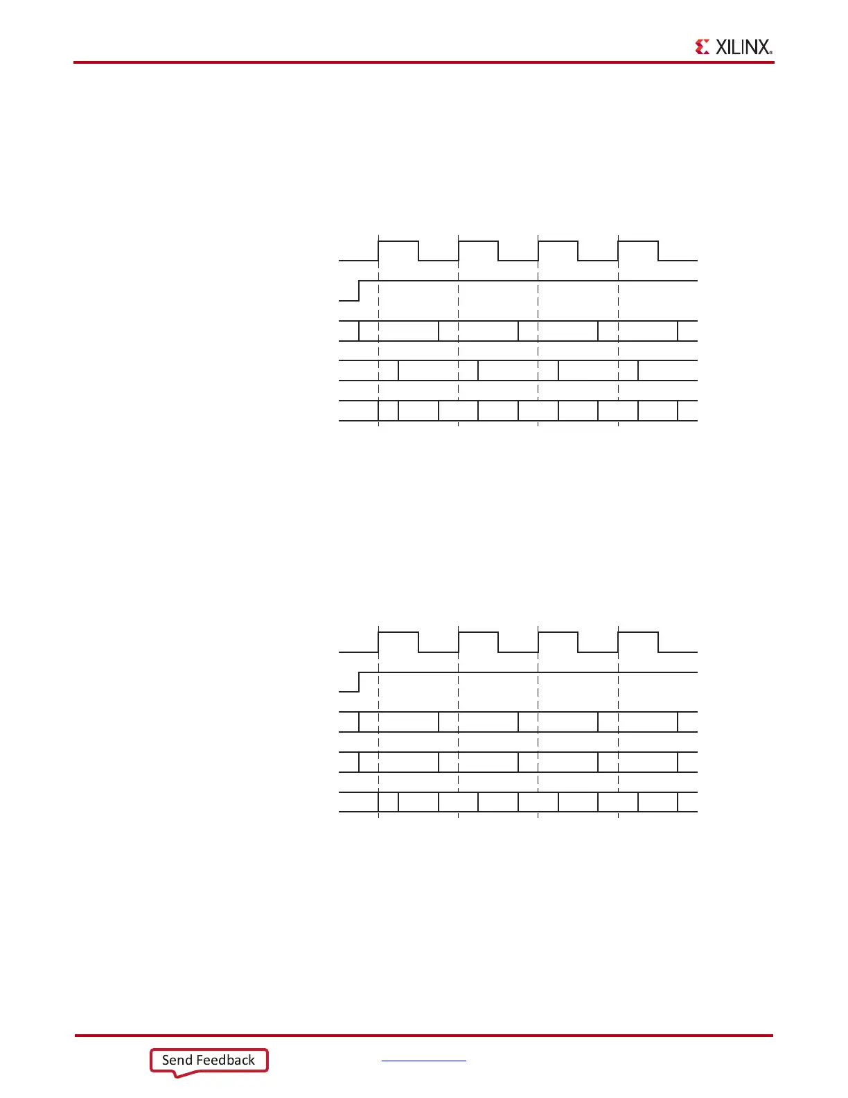
OPPOSITE_EDGE Mode
In OPPOSITE_EDGE mode, both the edges of the clock (CLK) are used to capture the data
from the FPGA logic at twice the throughput. This structure is similar to the Virtex-6 FPGA
implementation. Both outputs are presented to the data input or 3-state control input of the
IOB. The timing diagram of the output DDR using the OPPOSITE_EDGE mode is shown
in Figure 2-18.
SAME_EDGE Mode
In SAME_EDGE mode, data can be presented to the IOB on the same clock edge.
Presenting the data to the IOB on the same clock edge avoids setup time violations and
allows the user to perform higher DDR frequency with minimal register to register delay,
as opposed to using the CLB registers. Figure 2-19 shows the timing diagram of the output
DDR using the SAME_EDGE mode.
Clock Forwarding
Output DDR can forward a copy of the clock to the output. This is useful for propagating
a clock and DDR data with identical delays, and for multiple clock generation, where every
clock load has a unique clock driver. This is accomplished by tying the D1 input of the
ODDR primitive High, and the D2 input Low. Xilinx recommends using this scheme to
forward clocks from the FPGA logic to the output pins.
X-Ref Target - Figure 2-1 8
Figure 2-18: Output DDR Timing in OPPOSITE_EDGE Mode
ug471_c2_16_011811
CLK
OCE
OQ
D1
D2
D1A D2A D1B
D1A D1B D1C D1D
D2A D2B D2C D2D
D2B
D1C D2C D1D
X-Ref Target - Figure 2-1 9
Figure 2-19: Output DDR Timing in SAME_EDGE Mode
ug471_c2_17_011811
CLK
OCE
OQ
D1
D2
D1A D2A D1B
D1A D1B D1C D1D
D2A D2B D2C D2D
D2B
D1C D2C D1D