156 www.xilinx.com 7 Series FPGAs SelectIO Resources User Guide
UG471 (v1.10) May 8, 2018
Chapter 3: Advanced SelectIO Logic Resources
4. The SLAVE uses the ports Q3 to Q8 as outputs.
5. DATA_WIDTH applies to both MASTER and SLAVE in Figure 3-8.
ISERDESE2 Latencies
When the ISERDESE2 interface type is MEMORY, the latency through the OCLK stage is
one CLKDIV cycle. However, the total latency through the ISERDESE2 depends on the
phase relationship between the CLK and the OCLK clock inputs. When the ISERDESE2
interface type is NETWORKING, the latency is two CLKDIV cycles. See Figure 3-12,
page 160 for a visualization of latency in networking mode. The extra CLKDIV cycle of
latency in networking mode (compared to memory mode) is due to the Bitslip submodule.
The latency in MEMORY_QDR and MEMORY_DDR3 is two CLKDIV cycles.
Dynamic Clock Inversions
The dynamic clock inversion pins DYNCLKSEL and DYNCLKDIVSEL when used in
conjunction with DYN_CLK_SEL_EN and DYN_CLKDIV_SEL_EN respectively can
enable the user to dynamically switch the polarity of the respective clock source. This
operation causes the clock going into ISERDESE2 to switch asynchronously and will likely
cause the ISERDESE2 to produce erroneous data until the ISERDESE2 is reset. This
operation can only be supported in MEMORY_QDR and MEMORY_DDR3 mode.
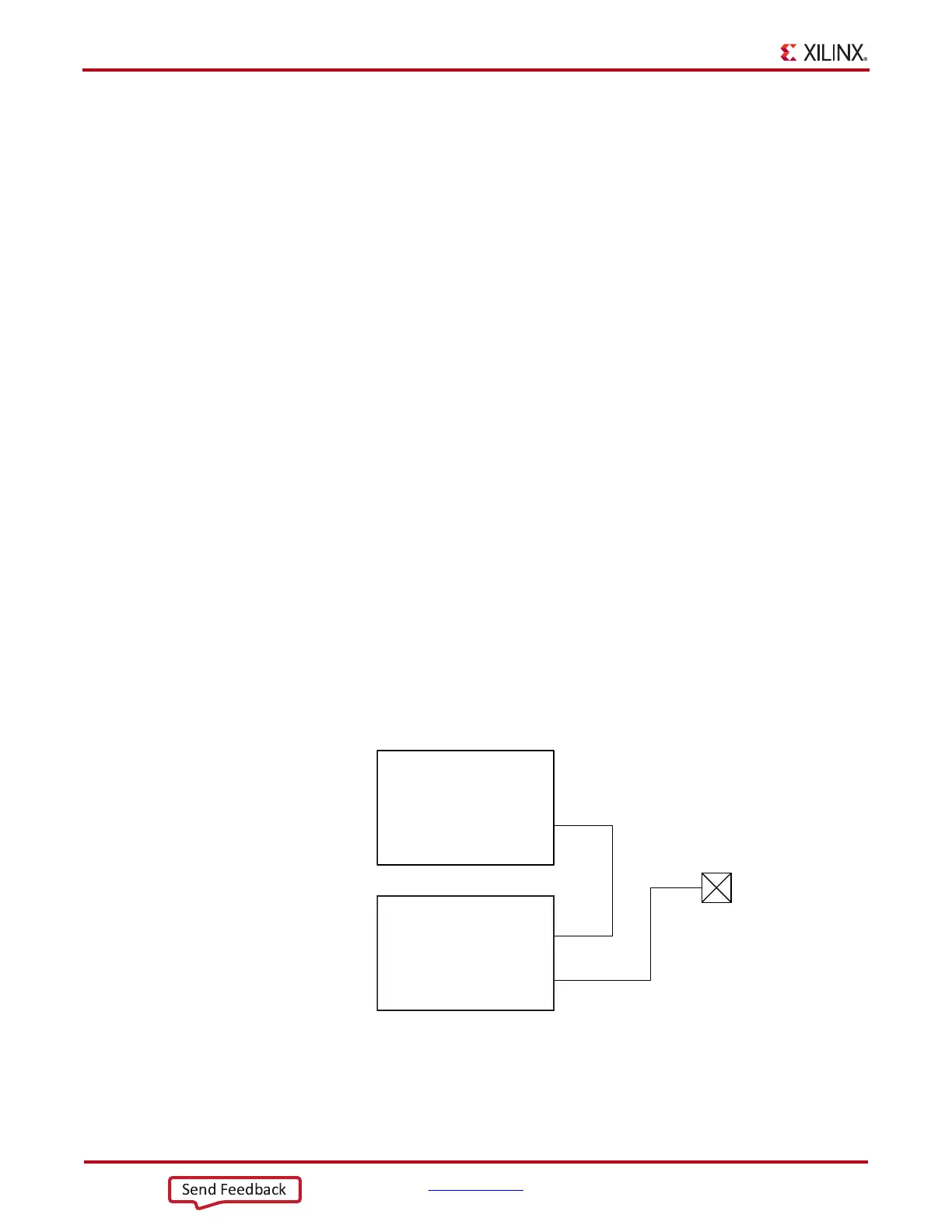
ISERDESE2 Feedback from OSERDESE2
The OFB port in the ISERDESE2 and OSERDESE2 can be used to feed the data transmitted
on the OSERDESE2 back to the ISERDESE2 (Figure 3-9). This feature is enabled when the
attribute OFB_USED = TRUE. The OSERDESE2 and ISERDESE2 must have the same
DATA_RATE and DATA_WIDTH setting for the feedback to give the correct data. When
using the ISERDESE2 and OSERDESE2 in width expansion mode only, connect the master
OSERDESE2 to the master ISERDESE2.
By using the ISERDESE2 as a feedback port, it can not be used as an input for external data.
X-Ref Target - Figure 3-9
Figure 3-9: ISERDESE2 and OSERDESE2 Connected via the OFB Port
ISERDESE2
OSERDESE2
OFB
OFB
OQ
ug471_c3_09_012211