7 Series FPGAs SelectIO Resources User Guide www.xilinx.com 31
UG471 (v1.10) May 8, 2018
7 Series FPGA DCI—Only available in the HP I/O banks
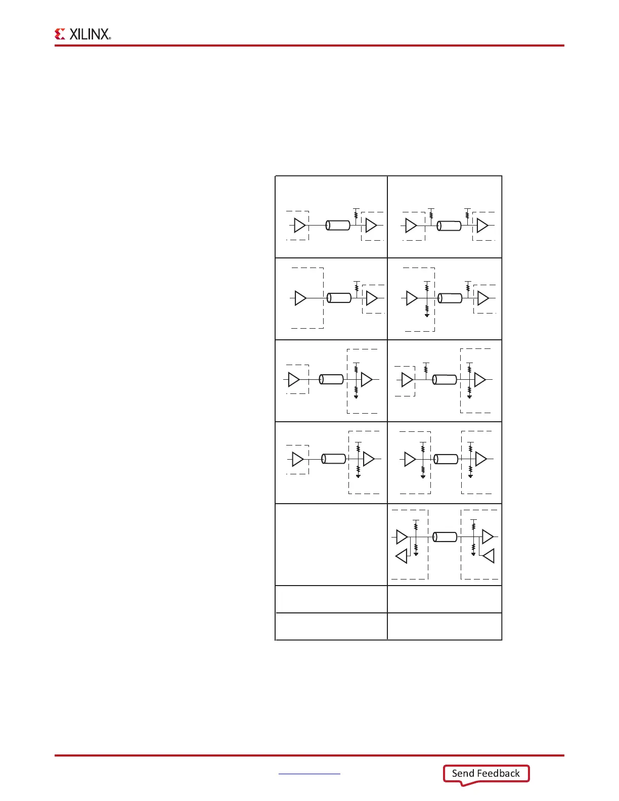
DCI Usage Examples
• Figure 1-13 provides examples illustrating the use of the HSTL_I_DCI and
HSTL_II_DCI I/O standards.
• Figure 1-14 provides examples illustrating the use of the SSTL18_I_DCI and
SSTL18_II_DCI I/O standards.
X-Ref Target - Figure 1-1 3
Figure 1-13: HSTL DCI Usage Examples
RR
2R
2R
R
2R
R
2R
2R
2R
2R
2R
UG471_c1_15_011811
Conventional
DCI Transmit
Conventional
Receive
Conventional
Transmit
DCI Receive
DCI Transmit
DCI Receive
Bidirectional
Reference
Resistor
Recommended
Z
0
VRN = VRP = 2R = 2Z
0
50Ω
VRN = VRP = 2R = 2Z
0
50Ω
HSTL_I HSTL_II
N/A
Z
0
R
R
2R
2R
2R
2R
Z
0
Z
0
Z
0
Z
0
Z
0
Z
0
Z
0
7 Series FPGA
HP Bank DCI
7 Series FPGA
HP Bank DCI
7 Series FPGA
HP Bank DCI
7 Series FPGA
HP Bank DCI
7 Series FPGA
HP Bank DCI
7 Series FPGA
HP Bank DCI
7 Series FPGA
HP Bank DCI
7 Series FPGA
HP Bank DCI
7 Series FPGA
HP Bank DCI
Z
0
2R
2R
2R
2R
V
CCO
/2
V
CCO
/2
V
CCO
/2
V
CCO
/2
V
CCO
/2 V
CCO
/2
V
CCO
V
CCO
V
CCO
V
CCO
V
CCO
V
CCO
V
CCO
V
CCO
Notes:
1. Z
0
is the recommended PCB trace impedance.