7 Series FPGAs SelectIO Resources User Guide www.xilinx.com 171
UG471 (v1.10) May 8, 2018
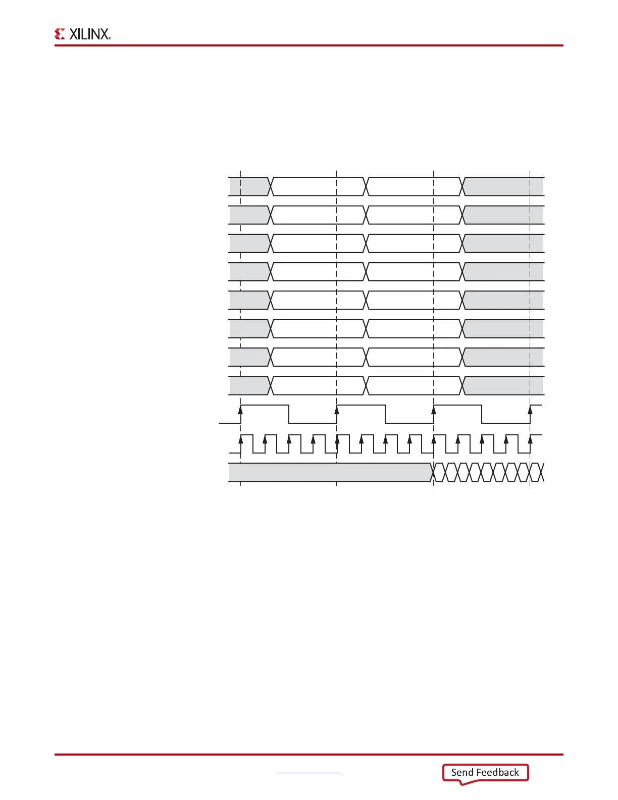
Output Parallel-to-Serial Logic Resources (OSERDESE2)
Timing Characteristics of 8:1 DDR Serialization
Figure 3-17 illustrates the timing of an 8:1 DDR data serialization. All eight of the bits are
connected to D1–D8 of the master OSERDESE2 in contrast to previous generations where
cascading was required.
Clock Event 1
On the rising edge of CLKDIV, the word ABCDEFGH is driven from the FPGA logic to the
D1–D8 inputs of the OSERDESE2.
Clock Event 2
On the rising edge of CLKDIV, the word ABCDEFGH is sampled into the OSERDESE2
from the D1–D8.
Clock Event 3
The data bit A appears at OQ four CLK cycles after ABCDEFGH is sampled into the
OSERDESE2. This latency is consistent with the Table 3-11 listing of a 8:1 DDR mode
OSERDESE2 latency of four CLK cycles.
The second word IJKLMNOP is sampled into the OSERDESE2 from the D1–D8.
X-Ref Target - Figure 3-17
Figure 3-17: OSERDESE2 Data Flow and Latency in 8:1 DDR Mode
Clock
Event 1
UG471_c3_17_111011
Master.D1
Master.D2
Master.D3
Master.D4
Master.D5
Master.D6
Master.D7
Master.D8
AI
BJ
CK
DL
EM
FN
GO
HP
CLKDIV
CLK
ABCDEFGHI
OQ
Clock
Event 2
Clock
Event 3
Clock
Event 4
 Loading...

