88 www.xilinx.com 7 Series FPGAs SelectIO Resources User Guide
UG471 (v1.10) May 8, 2018
Chapter 1: SelectIO Resources
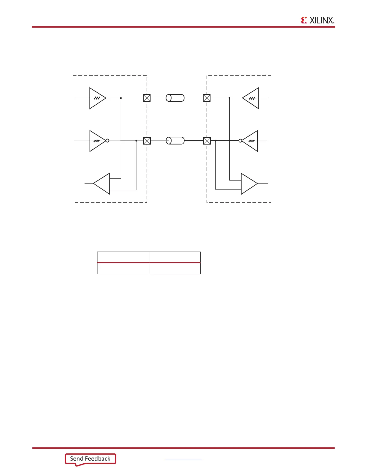
Figure 1-69 shows a sample circuit illustrating a board topology (with no termination) for
differential HSUL_12 with bidirectional DCI signalling.
MOBILE_DDR (Low Power DDR)
The MOBILE_DDR standard is for LPDDR and Mobile DDR memory buses.
MOBILE_DDR is defined by the JEDEC I/O standard JESD209A. It is a 1.8V single-ended
I/O standard that eliminates the need for V
REF
and V
TT
voltage supplies. 7 series FPGAs
support this standard for single-ended signaling and differential outputs. The differential
outputs drive the CK/CK# pins.
The differential (DIFF_) version uses complementary single-ended drivers for outputs,
and differential receivers for inputs.
Summary of Memory Interface IOSTANDARDs and Attributes Supported
Table 1-40 lists the available 7 series FPGA single-ended HSTL, SSTL, HSUL, and
MOBILE_DDR I/O standards and attributes supported.
Table 1-41 lists the available 7 series FPGA differential HSTL, SSTL, HSUL, and
MOBILE_DDR I/O standards and attributes supported.
Table 1-42 lists the SLEW attribute for the 7 series FPGA single-ended and differential
HSTL, SSTL, HSUL, and MOBILE_DDR I/O standards.
X-Ref Target - Figure 1-69
Figure 1-69: Differential HSUL_12 with DCI Bidirectional Signalling
Z
0
IOB
IOB
DIFF_HSUL_12_DCI DIFF_HSUL_12_DCI
+
–
DCI
DIFF_HSUL_12_DCI
ug471_c1_59_011811
Z
0
DIFF_HSUL_12_DCI
DIFF_HSUL_12_DCI DIFF_HSUL_12_DCI
+
–
R
0
= 50Ω
R
0
= 50Ω
R
0
= 50Ω
R
0
= 50Ω
Table 1-39: Available I/O Bank Type
HR HP
Available N/A