7 Series FPGAs SelectIO Resources User Guide www.xilinx.com 163
UG471 (v1.10) May 8, 2018
Output Parallel-to-Serial Logic Resources (OSERDESE2)
OSERDESE2 Ports
Table 3-6 lists the available ports in the OSERDESE2 primitive.
Data Path Output - OQ
The OQ port is the data output port of the OSERDESE2 module. Data at the input port D1
will appear first at OQ. This port connects the output of the data parallel-to-serial
converter to the data input of the IOB. This port can not drive the ODELAYE2; the OFB pin
must be used.
Output Feedback from OSERDESE2 - OFB
The output feedback port (OFB) is the serial (high-speed) data output port of the
OSERDESE2 for use with the ODELAYE2 primitive, or the OFB port can be used to send
out serial data to the ISERDESE2. See Output Feedback.
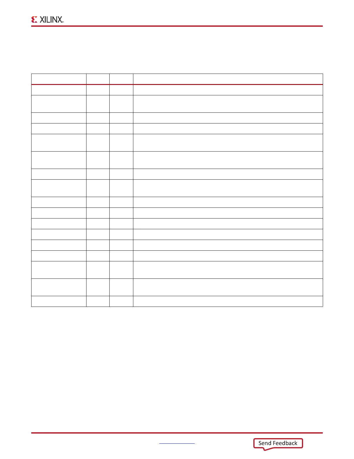
Table 3-6: OSERDESE2 Port List and Definitions
Port Name Type Width Description
OQ Output 1 Data path output to IOB only. See Data Path Output - OQ.
OFB Output 1 Data path output feedback to ISERDESE2 or connection to ODELAYE2. See
Output Feedback.
TQ Output 1 3-state control output to IOB. See 3-state Control Output - TQ.
TFB Output 3-state control output to fabric. See 3-state Control Output - TFB.
SHIFTOUT1 Output 1 Carry output for data width expansion. Connect to SHIFTIN1 of master
OSERDESE2. See OSERDESE2 Width Expansion.
SHIFTOUT2 Output 1 Carry output for data width expansion. Connect to SHIFTIN2 of master
OSERDESE2. See OSERDESE2 Width Expansion.
CLK Input 1 High-speed clock input. See High-Speed Clock Input - CLK.
CLKDIV Input 1 Divided clock input. Clocks delay element, deserialized data, and CE unit.
See Divided Clock Input - CLKDIV.
D1 to D8 Input 1 (each) Parallel data inputs. See Parallel Data Inputs - D1 to D8.
TCE Input 1 3-state clock enable. See 3-state Signal Clock Enable - TCE.
OCE Input 1 Output data clock enable. See Output Data Clock Enable - OCE.
TBYTEIN Input 1 Byte group 3-state input.
TBYTEOUT Output 1 Byte group 3-state output.
RST Input 1 Active High reset.
SHIFTIN1 Input 1 Carry input for data width expansion. Connect to SHIFTOUT1 of slave
OSERDESE2. See OSERDESE2 Width Expansion.
SHIFTIN2 Input 1 Carry input for data width expansion. Connect to SHIFTOUT2 of slave
OSERDESE2. See OSERDESE2 Width Expansion.
T1 to T4 Input 1 (each) Parallel 3-state inputs. See Parallel 3-state Inputs - T1 to T4.
 Loading...

