28 www.xilinx.com 7 Series FPGAs SelectIO Resources User Guide
UG471 (v1.10) May 8, 2018
Chapter 1: SelectIO Resources
DCI and 3-state DCI (T_DCI)
The class-I driver versions of the SSTL and HSTL I/O standards are only supported for
unidirectional signaling; they can only be assigned to input-only or output-only pins in a
design, not bidirectional pins. The DCI versions of class-I SSTL and HSTL I/O standards
only have internal split-termination resistors present on inputs (not outputs). The class-II
driver versions of SSTL and HSTL I/O standards are supported for bidirectional and
unidirectional signaling; they can be assigned to input, output, or bidirectional pins in a
design. The DCI versions of class-II SSTL and HSTL I/O standards always have internal
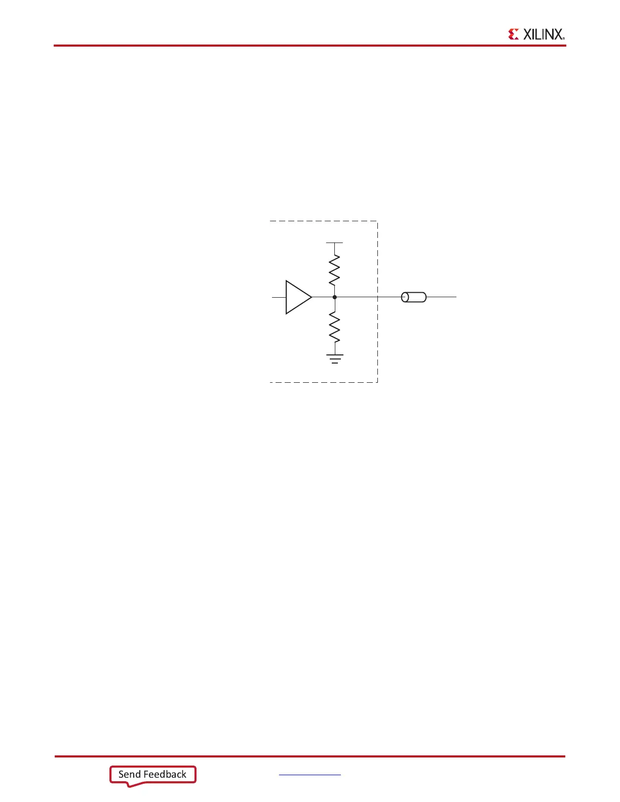
split-termination resistors present on input, outputs, or bidirectional pins. Figure 1-12
illustrates a driver with split termination inside a 7 series device.
When the split-termination is present while driving, DCI only controls the impedance of
the termination, but not the driver. However, many applications can benefit from having
the split-termination resistors turned off whenever the pin is driving. The 3-state DCI
(T_DCI) standards were designed to meet this requirement by turning off the
split-termination resistors whenever the output buffer is driving, and turning on the
split-termination resistors when the output is in 3-state (such as when receiving or in an
idle state). The T_DCI standards can only be assigned to bidirectional pins. For
unidirectional input pins, the DCI version of the standard can be assigned. For
unidirectional output pins, either the non-DCI or the DCI version can be assigned.
X-Ref Target - Figure 1-1 2
Figure 1-12: Driver with Termination to V
CCO
/2 Using DCI Split Termination
(External Resistors on VRN, VRP = 2R)
2R
2R
UG471_c1_14_011811
V
CCO
IOB
Z
0
7 Series FPGA HP Bank DCI