148 www.xilinx.com 7 Series FPGAs SelectIO Resources User Guide
UG471 (v1.10) May 8, 2018
Chapter 3: Advanced SelectIO Logic Resources
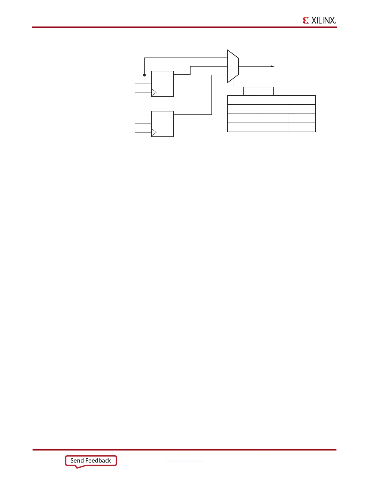
When NUM_CE = 1, the CE2 input is not used, and the CE1 input is an active High clock
enable connected directly to the input registers in the ISERDESE2. When NUM_CE = 2, the
CE1 and CE2 inputs are both used, with CE1 enabling the ISERDESE2 for ½ of a CLKDIV
cycle, and CE2 enabling the ISERDESE2 for the other ½. The internal clock enable signal
ICE shown in Figure 3-4 is derived from the CE1 and CE2 inputs. ICE drives the clock
enable inputs of registers FF0, FF1, FF2, and FF3 shown in Figure 3-5, page 152. The
remaining registers in Figure 3-5, page 152 do not have clock enable inputs.
The clock enable module functions as a 2:1 serial-to-parallel converter, clocked by CLKDIV.
The clock enable module is needed specifically for bidirectional memory interfaces when
ISERDESE2 is configured for 1:4 deserialization in DDR mode. When the attribute
NUM_CE = 2, the clock enable module is enabled and both CE1 and CE2 ports are
available. When NUM_CE = 1, only CE1 is available and functions as a regular clock
enable.
High-Speed Clock Input - CLK
The high-speed clock input (CLK) is used to clock in the input serial data stream.
High-Speed Clock Input - CLKB
The high-speed secondary clock input (CLKB) is used to clock in the input serial data
stream. In any mode other than MEMORY_QDR, connect CLKB to an inverted version of
CLK. In MEMORY_QDR mode CLKB should be connected to a unique, phase shifted
clock. See ISERDESE2 Clocking Methods.
Divided Clock Input - CLKDIV
The divided clock input (CLKDIV) is typically a divided version of CLK (depending on the
width of the implemented deserialization). It drives the output of the serial-to-parallel
converter, the Bitslip submodule, and the CE module.
Serial Input Data from IOB - D
The serial input data port (D) is the serial (high-speed) data input port of the ISERDESE2.
This port works in conjunction only with the 7 series FPGA IOB resource. See Using D and
DDLY in the ISERDESE2.
X-Ref Target - Figure 3-4
Figure 3-4: Input Clock Enable Module
D
AR
CE1R
ICE
NUM_CE ICECLKDIV
1 CE1X
2 CE2R0
2 CE1R1
(To ISERDESE2 Input Registers)
CE1 Q
RST
CLKDIV
D
AR
CE2R
CE2 Q
RST
CLKDIV
UG471_c3_04_080310