7 Series FPGAs SelectIO Resources User Guide www.xilinx.com 147
UG471 (v1.10) May 8, 2018
Input Serial-to-Parallel Logic Resources (ISERDESE2)
Combinatorial Output – O
The combinatorial output port (O) is an unregistered output of the ISERDESE2 module.
This output can come directly from the data input (D), or from the data input (DDLY) via
the IDELAYE2.
Bitslip Operation - BITSLIP
The BITSLIP pin performs a Bitslip operation synchronous to CLKDIV when asserted
(active High). Subsequently, the data seen on the Q1 to Q8 output ports will shift, as in a
barrel-shifter operation, one position every time Bitslip is invoked (DDR operation is
different from SDR). See BITSLIP Submodule for more details.
Clock Enable Inputs - CE1 and CE2
Each ISERDESE2 block contains an input clock enable module (Figure 3-4).
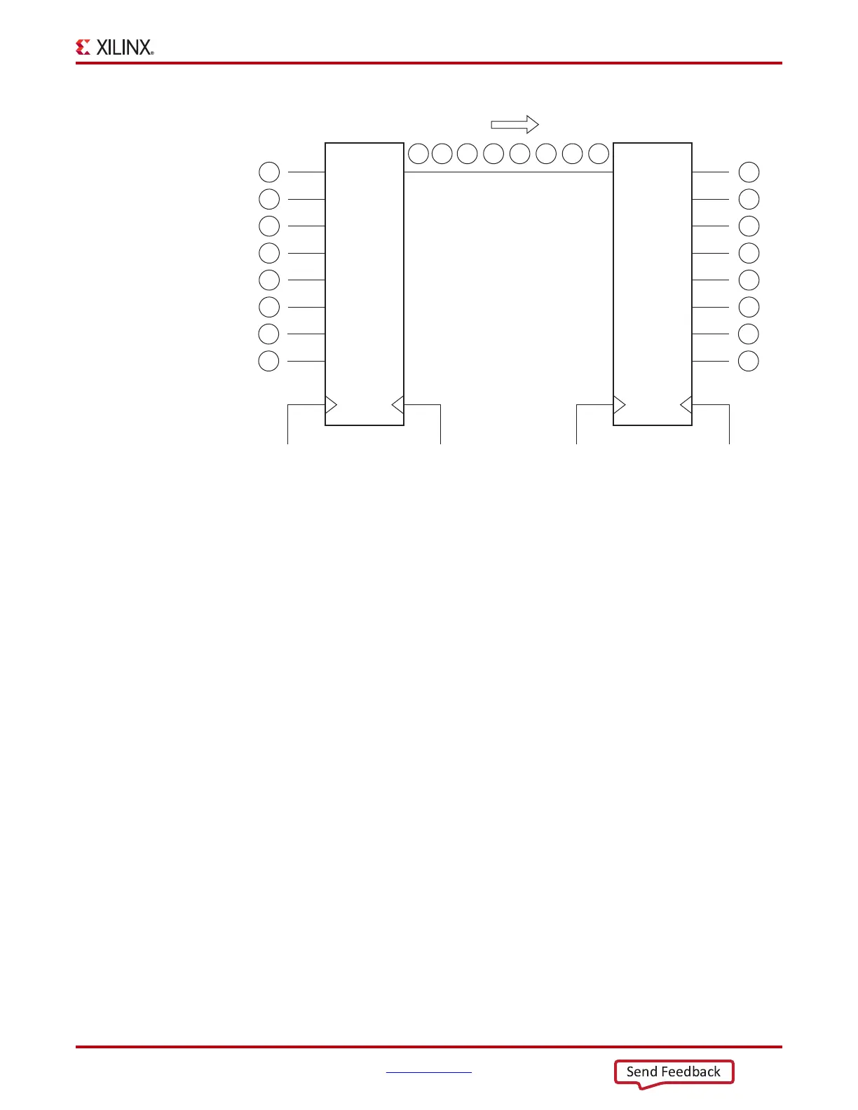
X-Ref Target - Figure 3-3
Figure 3-3: Bit Ordering on Q1–Q8 Outputs of ISERDESE2 Ports
FGH E
QD
OSERDESE2 ISERDESE2
Data Bits
D1
D C B A
A
D2
B
D3
C
D4
D
D5
E
D6
Q1
Q2
Q3
Q4
Q5
Q6
F
H
G
F
E
D
C
D7
G
D8
Q7
Q8
H
B
A
CLKDIV_TX
CLK_TX CLK_RX CLKDIV_RX
UG471_c3_03_120910