7 Series FPGAs SelectIO Resources User Guide www.xilinx.com 169
UG471 (v1.10) May 8, 2018
Output Parallel-to-Serial Logic Resources (OSERDESE2)
Note: In Table 3-11, the CLK and CLKDIV clock edges are normally not phase aligned. When the
edges of both clocks are phase aligned, the latency can vary by one cycle.
OSERDESE2 Timing Model and Parameters
This section discusses all timing models associated with the OSERDESE2 primitive.
Table 3-12 describes the function and control signals of the OSERDESE2 switching
characteristics in the 7 series FPGA data sheets.
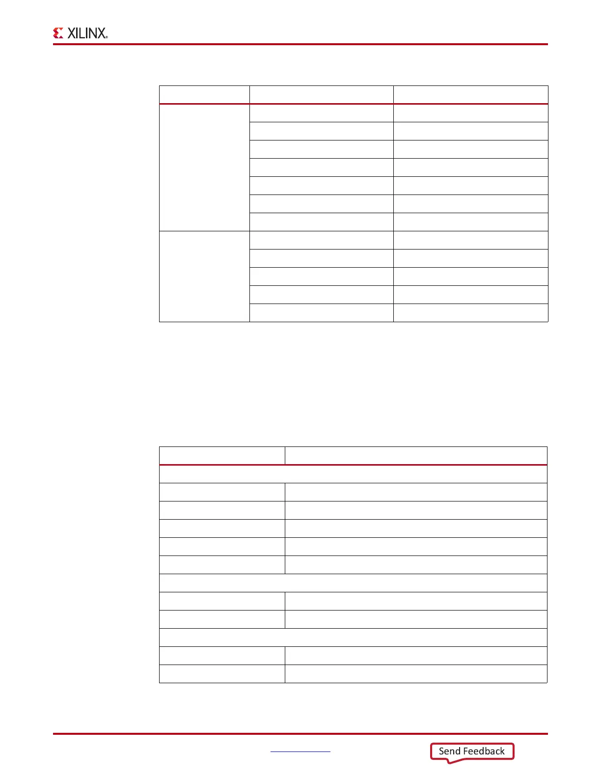
Table 3-11: OSERDESE2 Latencies
DATA_RATE DATA_WIDTH Latency
SDR
2:1 1 CLK cycle
3:1 2 CLK cycles
4:1 3 CLK cycles
5:1 4 CLK cycles
6:1 5 CLK cycles
7:1 6 CLK cycles
8:1 7 CLK cycles
DDR
4:1 2 CLK cycles
6:1 3 CLK cycles
8:1 4 CLK cycles
10:1 5 CLK cycles
14:1 5 CLK cycles
Table 3-12: OSERDESE2 Switching Characteristics
Symbol Description
Setup/Hold
T
OSDCK_D
/T
OSCKD_D
D input Setup/Hold with respect to CLKDIV
T
OSDCK_T
/T
OSCKD_T
T input Setup/Hold with respect to CLK
T
OSDCK_T
/T
OSCKD_T
T input Setup/Hold with respect to CLKDIV
T
OSCCK_OCE
/T
OSCKC_OCE
OCE input Setup/Hold with respect to CLK
T
OSCCK_TCE
/T
OSCKC_TCE
TCE input Setup/Hold with respect to CLK
Sequential Delays
T
OSCKO_OQ
Clock to Out from CLK to OQ
T
OSCKO_TQ
Clock to Out from CLK to TQ
Combinatorial
T
OSCO_OQ
Asynchronous Reset to OQ
T
OSCO_TQ
Asynchronous Reset to TQ