48 www.xilinx.com 7 Series FPGAs SelectIO Resources User Guide
UG471 (v1.10) May 8, 2018
Chapter 1: SelectIO Resources
•All V
REF
-based inputs such as HSLVDCI, SSTL, HSTL, and HSUL
• All input and bidirectional primitives
The IBUF_LOW_PWR attribute allows an optional trade-off between performance and
power. The change in the performance is reflected in the delay through the input buffer
and can be measured in the static timing report for the design. The change in power can be
estimated using the XPower Estimator (XPE) or XPower Analyzer (XPA) tools.
This attribute is set to TRUE by default, which implements the input buffer in the
lower-power mode rather than the higher-performance mode. The IBUF_LOW_PWR
attribute is applied to the I/O buffer instance and uses the following syntax in the UCF file:
INST <I/O_BUFFER_INSTANTIATION_NAME> IBUF_LOW_PWR=[TRUE|FALSE];
Output Slew Rate Attributes
A variety of attribute values provide the option of choosing the desired slew rate for I/O
output buffers. For LVCMOS, LVTTL, SSTL, HSTL, MOBILE_DDR, and HSUL output
buffers, including the differential versions, the desired slew rate can be specified with the
SLEW attribute.
It might be important to specify FAST slew rate for high-performance applications such as
high-frequency memory interfaces. However, faster slew rates can also lead to reflections
or increased noise issues if not properly designed (such as with terminations, transmission
line impedance continuity, and cross-coupling).
The allowed values for the SLEW attribute are:
• SLEW = SLOW (Default)
• SLEW = FAST
The SLEW attribute uses the following syntax in the UCF file:
INST <I/O_BUFFER_INSTANTIATION_NAME> SLEW = "<SLEW_VALUE>";
By default, the slew rate for each output buffer is set to SLOW. This is the default used to
minimize the power bus transients when switching non-critical signals.
Output Drive Strength Attributes
For LVCMOS and LVTTL output buffers (OBUF, OBUFT, and IOBUF), the desired drive
strength (in mA) can be specified with the DRIVE attribute.
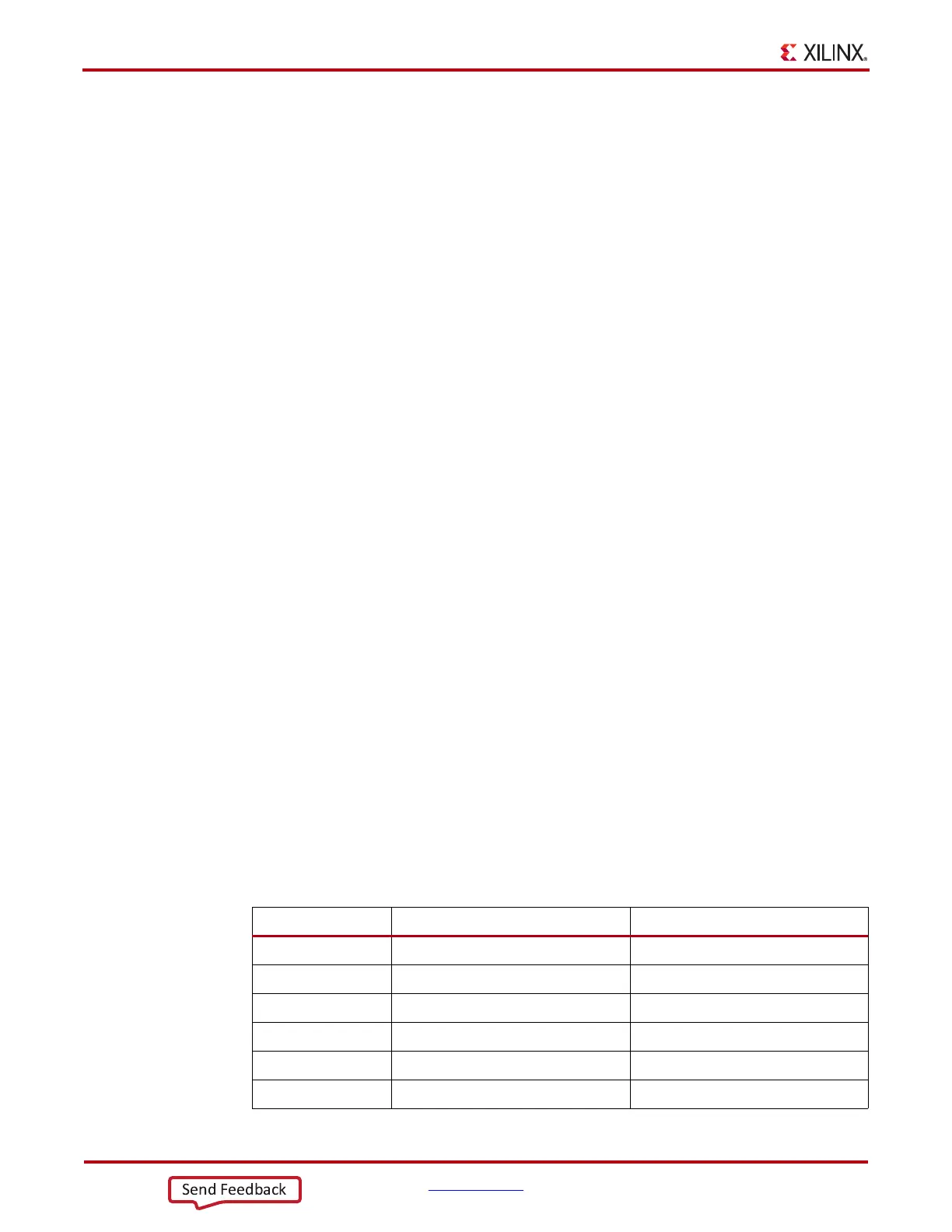
The allowed values for the DRIVE attribute are shown in Table 1-8. The default DRIVE
value is 12.
Table 1-8: Allowed Values for the DRIVE Attribute
Standard HR Bank Current Drive (mA) HP Bank Current Drive (mA)
LVCMOS12 4, 8, or 12 2, 4, 6, or 8
LVCMOS15 4, 8, 12, or 16 2, 4, 6, 8, 12, or 16
LVCMOS18 4, 8, 12, 16, or 24 2, 4, 6, 8, 12, or 16
LVCMOS25 4, 8, 12, or 16 N/A
LVCMOS33 4, 8, 12, or 16 N/A
LVTTL 4, 8, 12, 16, or 24 N/A