7 Series FPGAs SelectIO Resources User Guide www.xilinx.com 139
UG471 (v1.10) May 8, 2018
Output Delay Resources (ODELAY)—Not Available in HR Banks
• Loadable variable delay mode (ODELAY_TYPE = VAR_LOAD)
In addition to having the same functionality of (ODELAY_TYPE = VARIABLE) in this
mode the ODELAY tap can be loaded via the 5-input bits CNTVALUEIN<4:0> from
the FPGA logic. When LD is pulsed the value present at CNTVALUEIN<4:0> will be
the new tap value. As a results of this functionality the ODELAY_VALUE attribute is
ignored. When used in this mode, the IDELAYCTRL primitive must be instantiated.
See IDELAYCTRL Usage and Design Guidelines for more details. The control pins
being used in VAR_LOAD mode are described in Table 2-7.
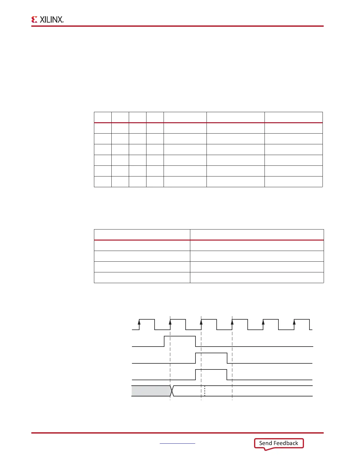
ODELAY Timing
Table 2-17 shows the ODELAY switching characteristics.
Figure 2-26 shows an ODELAYE2 (ODELAY_TYPE = VARIABLE, ODELAY_VALUE = 0,
and DELAY_SRC = CLKIN/ODATAIN) timing diagram.
Table 2-16: Control Pin when ODELAY_TYPE = VAR_LOAD
C LD CE INC CNTVALUEIN CNTVALUEOUT TAP Setting
0 x x x x No Change No Change
1 1 x x CNTVALUEIN CNTVALUEIN CNTVALUEIN
1 0 0 x x No Change No Change
1011 x Current Value +1 Current Value +1
1010 x Current Value –1 Current Value –1
1000 0 No Change No Change
Table 2-17: ODELAY Switching Characteristics
Symbol Description
T
IDELAYRESOLUTION
IDELAY tap resolution
T
ICECK
/T
ICKCE
CE pin Setup/Hold with respect to C
T
IINCCK
/T
ICKINC
INC pin Setup/Hold with respect to C
T
IRSTCK
/T
ICKRST
LD pin Setup/Hold with respect to C
X-Ref Target - Figure 2-2 6
Figure 2-26: ODELAY Timing Diagram (VARIABLE Mode)
UG471_c2_24_011811
LD
C
123
CE
INC
DATAO U T
Tap 0 Tap 1
 Loading...

