140 www.xilinx.com 7 Series FPGAs SelectIO Resources User Guide
UG471 (v1.10) May 8, 2018
Chapter 2: SelectIO Logic Resources
Clock Event 1
On the rising edge of C, a reset is detected (LD is High), causing the output DATAOUT to
select tap 0 as the output from the 31-tap chain.
Clock Event 2
A pulse on CE and INC is captured on the rising edge of C. This indicates an increment
operation. The output changes without glitches from tap 0 to tap 1. See Stability after an
Increment/Decrement Operation.
Clock Event 3
CE and INC are no longer asserted, thus completing the increment operation. The output
remains at tap 1 indefinitely until there is further activity on the LD, CE, or INC pins.
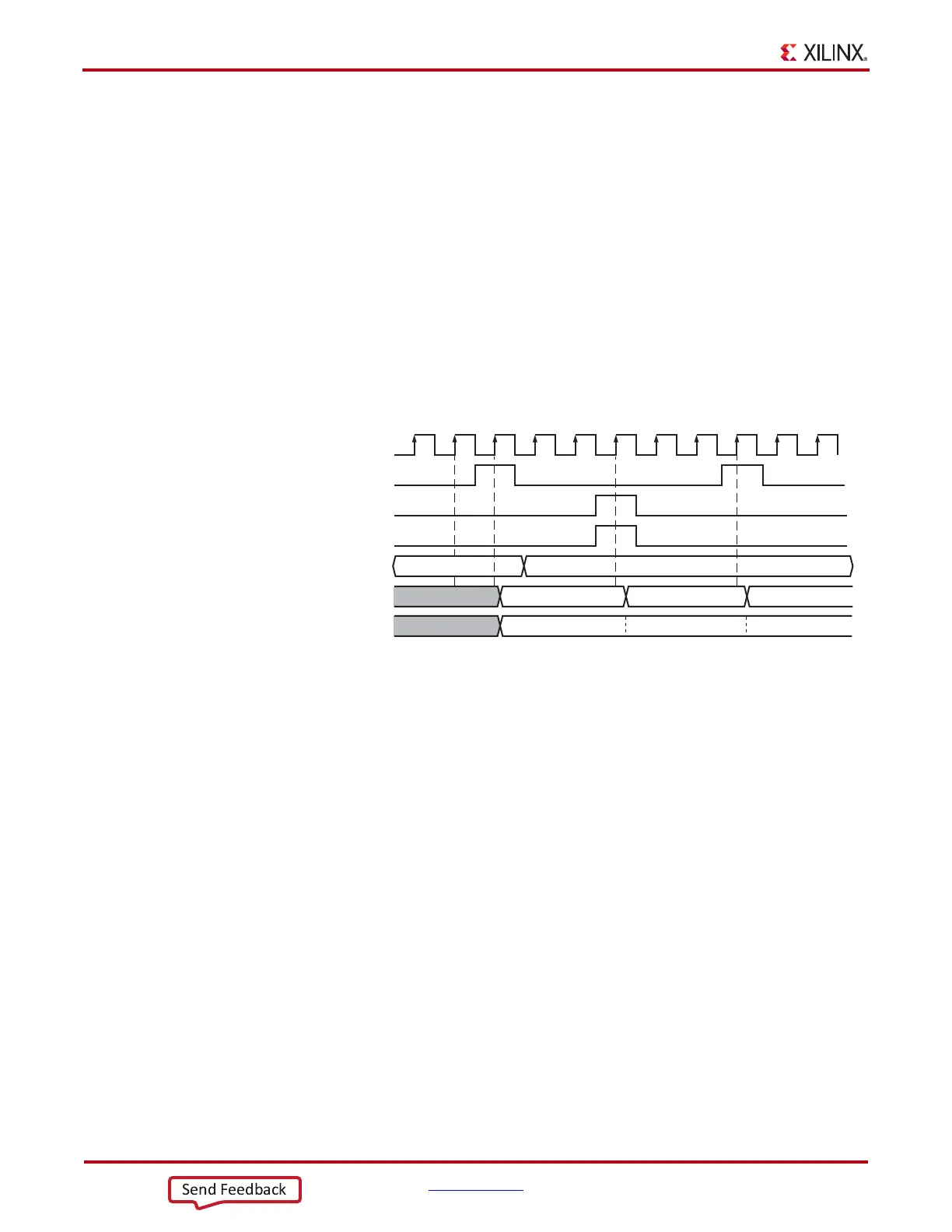
Figure 2-27 shows an ODELAY timing diagram.
Clock Event 0
Before LD is pulsed the tap setting and CNTVALUEOUT are at an unknown value.
Clock Event 1
On the rising edge of C, LD is detected as High causing the output DATAOUT to be equal
to the CNTINVALUE, and changing the tap setting to tap 2. The CNTVALUEOUT is
updated to represent the new tap value.
Clock Event 2
A pulse on CE and INC are captured on the rising edge of C. This indicates an increment
operation. The output changes without glitches from tap 2 to tap 3. The CNTVALUEOUT
is updated to represent the new tap value.
Clock Event 3
On the rising edge of C, a LD is detected causing the output DATAOUT to be equal to the
CNTINVALUE. The CNTVALUEOUT shows the value of the tap setting. The output will
remain at tap 10 indefinitely until there is further activity on the LD, CE, or INC pins.
X-Ref Target - Figure 2-2 7
Figure 2-27: ODELAY in VAR_LOAD Timing Diagram
C
LD
INC
CE
CNTVALUEIN
CNTVALUEOUT
DATAO UT
5’b00010 5’b00011 5’b01010
5’b00010 5’b01010
01 2 3
Tap 2 Tap 3 Tap 10
UG471_c2_25_011811