172 www.xilinx.com 7 Series FPGAs SelectIO Resources User Guide
UG471 (v1.10) May 8, 2018
Chapter 3: Advanced SelectIO Logic Resources
Clock Event 4
Between Clock Events 3 and 4, the entire word ABCDEFGH is transmitted serially on OQ,
a total of eight bits transmitted in one CLKDIV cycle.
The data bit I appears at OQ four CLK cycles after IJKLMNOP is sampled into the
OSERDESE2. This latency is consistent with the Table 3-11 listing of a 8:1 DDR mode
OSERDESE2 latency of four CLK cycles.
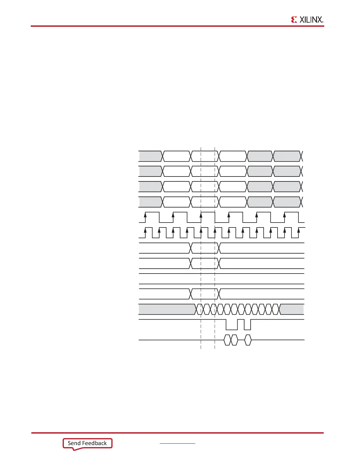
Timing Characteristics of 4:1 DDR 3-State Controller Serialization
The operation of a 3-state controller is illustrated in Figure 3-18. The example is a 4:1 DDR
case shown in a bidirectional system where the IOB must be frequently 3-stated.
Clock Event 1
T1, T2, and T4 are driven Low to release the 3-state condition. The serialization paths of
T1–T4 and D1–D4 in the OSERDESE2 are identical (including latency), such that the bits
EFGH are always aligned with the 0010 presented at the T1–T4 pins during Clock Event 1.
X-Ref Target - Figure 3-18
Figure 3-18: OSERDESE2 Data Flow and Latency in 4:1 DDR Mode
Clock
Event 1
UG471_c3_18_021914
D1 A E I
BFJ
CGK
D
10 1
10 1
111
1
AB CD EF GH
EF H
IJKL
01
HL
D2
D3
D4
CLKDIV
CLK
T1
T2
T3
T4
OQ
TQ
OBUFT.O
Clock
Event 2