78 www.xilinx.com 7 Series FPGAs SelectIO Resources User Guide
UG471 (v1.10) May 8, 2018
Chapter 1: SelectIO Resources
SSTL18, SSTL15, SSTL135, SSTL12
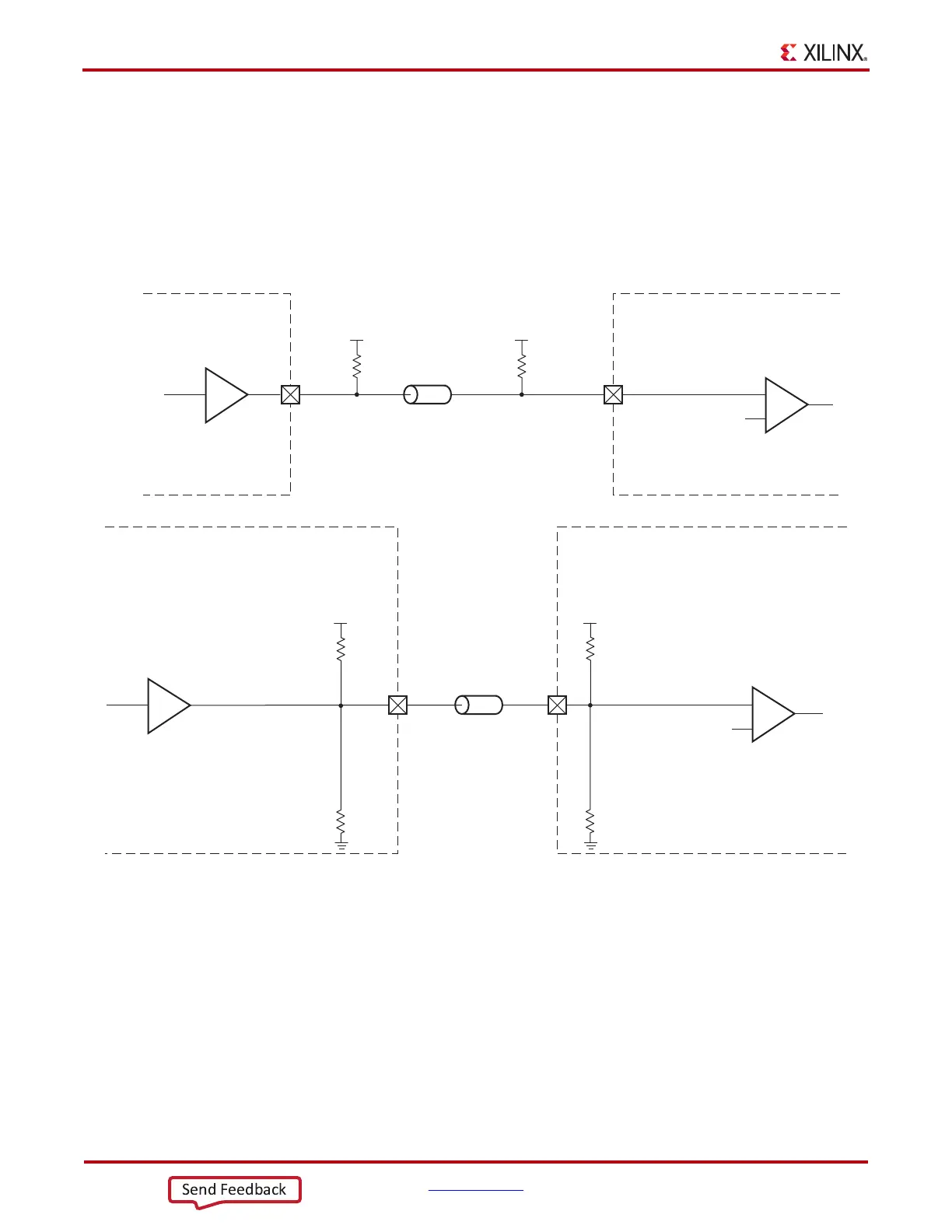
Figure 1-57 shows a sample circuit illustrating a unidirectional termination technique for
SSTL18, SSTL15, SSTL135, or SSTL12. In a specific circuit, all drivers and receivers must be
at the same voltage level (1.8V, 1.5V, 1.35V, or 1.2V); they are not interchangeable. Also
shown in Figure 1-57, only SSTL18_II_DCI has internal split-termination resistors present
in an output pin.
X-Ref Target - Figure 1-57
Figure 1-57: SSTL18, SSTL15, SSTL135, or SSTL12 Unidirectional Termination
Z
0
IOB
IOB
SSTL18_(I/II)
SSTL15(_R)
SSTL135(_R)
SSTL12
SSTL18_(I/II)
SSTL15(_R)
SSTL135(_R)
SSTL12
ug471_c1_47_121214
V
TT
=
0.9V for SSTL18_(I/II)
0.75V for SSTL15(_R)
0.675V for SSTL135(_R)
0.6V for SSTL12
R
P
= Z
0
= 50Ω
Z
0
IOB
IOB
SSTL18_(I/II)_DCI
SSTL15_DCI
SSTL135_DCI
SSTL12_DCI
SSTL18_(I/II)_DCI
SSTL15_DCI
SSTL135_DCI
SSTL12_DCI
V
CCO
=
1.8V for SSTL18_(I/II)_DCI
1.5V for SSTL15_DCI
1.35V for SSTL135_DCI
1.2V for SSTL12_DCI
V
CCO
=
1.8V for SSTL18_II_DCI
R
VRN
= 2Z
0
= 100Ω
R
VRP
= 2Z
0
= 100Ω
V
REF
=
0.9V for SSTL18_(I/II)
0.75V for SSTL15(_R)
0.675V for SSTL135(_R)
0.6V for SSTL12
V
REF
=
0.9V for SSTL18_(I/II)_DCI
0.75V for SSTL15_DCI
0.675V for SSTL135_DCI
0.6V for SSTL12_DCI
+
–
+
–
External Termination
DCI
R
VRN
= 2Z
0
= 100Ω
R
VRP
= 2Z
0
= 100Ω
V
TT
=
0.9V for SSTL18_II
R
P
= Z
0
= 50Ω