7 Series FPGAs SelectIO Resources User Guide www.xilinx.com 157
UG471 (v1.10) May 8, 2018
Input Serial-to-Parallel Logic Resources (ISERDESE2)
Using D and DDLY in the ISERDESE2
The D and DDLY pins are dedicated inputs to the ISERDESE2. The D input is a direct
connection to the IOB. The DDLY pin is a direct connection to the IDELAYE2. This allows
the user to either have a delayed or non-delayed version of the input to the registered
(Q1-Q8) or combinatorial path (O) output. The attribute IOBDELAY determines the input
applied to the ISERDESE2. Table 3-4 shows the result of each setting of the IOBDELAY
value when both D and DDLY are connected.
ISERDESE2 Timing Model and Parameters
Table 3-5 describes the function and control signals of the ISERDESE2 switching
characteristics in the 7 series FPGA data sheets.
Timing Characteristics
Figure 3-10 illustrates an ISERDESE2 timing diagram for the input data to the ISERDESE2.
The timing parameter names change for different modes (SDR/DDR). However, the
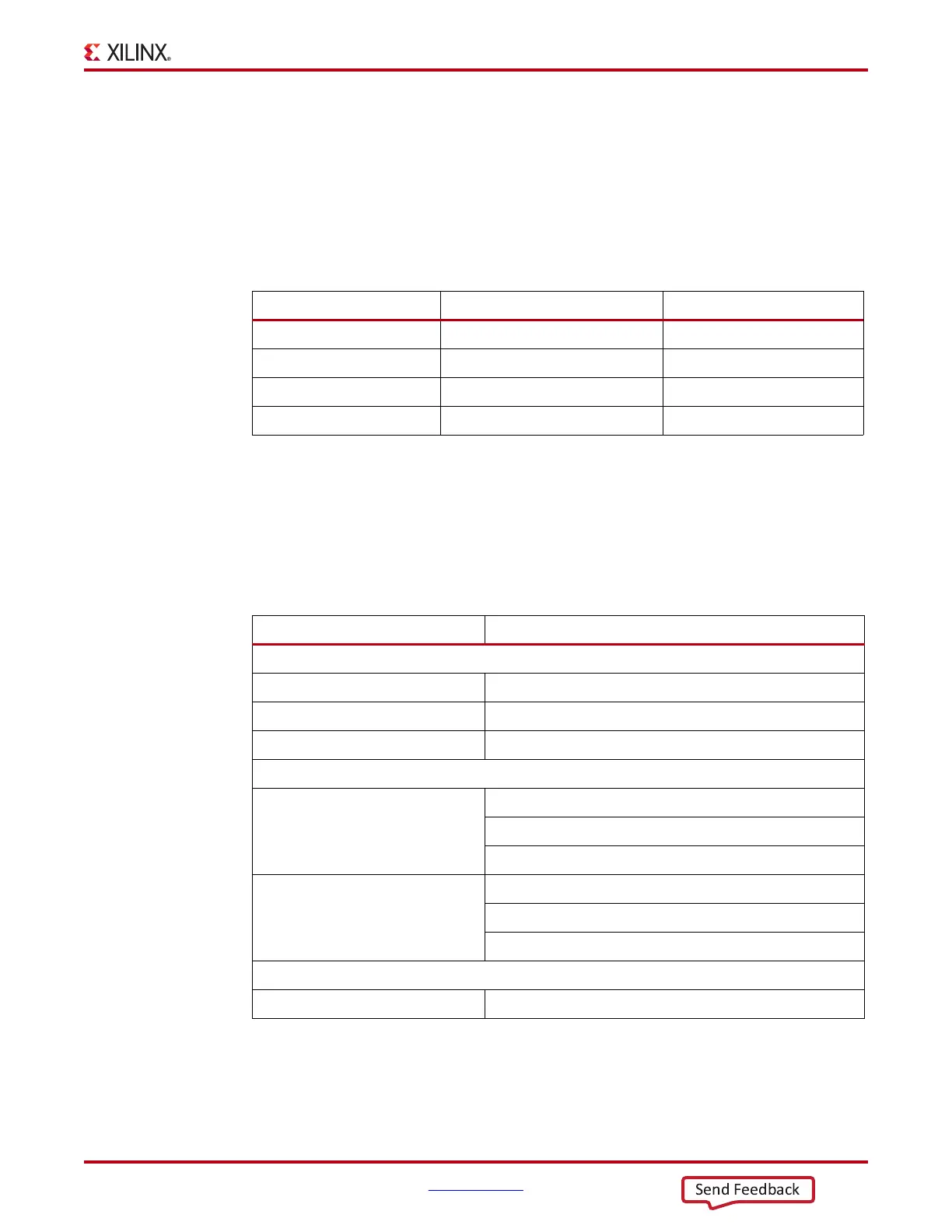
Table 3-4: IOBDELAY Attribute Value on the Associated IOBDELAY Block
(1)
IOBDELAY Value Combinatorial Output (O) Registered Output (Q1-Q8)
NONE D D
IBUF DDLY D
IFD D DDLY
BOTH DDLY DDLY
Notes:
1. When both D and DDLY are connected to ISERDESE2.
Table 3-5: ISERDESE2 Switching Characteristics
Symbol Description
Setup/Hold for Control Lines
T
ISCCK_BITSLIP
/ T
ISCKC_BITSLIP
BITSLIP pin Setup/Hold with respect to CLKDIV
T
ISCCK_CE
/T
ISCKC_CE
CE pin Setup/Hold with respect to CLKDIV (for CE1)
T
ISCCK_CE2
/T
ISCKC_CE2
CE pin Setup/Hold with respect to CLKDIV (for CE2)
Setup/Hold for Data Lines
T
ISDCK_D
/ T
ISCKD_D
D pin Setup/Hold with respect to CLK
D pin Setup/Hold with respect to CLK
D pin Setup/Hold with respect to CLK
T
ISDCK_DDR
/ T
ISCKD_DDR
D pin Setup/Hold with respect to CLK at DDR mode
D pin Setup/Hold with respect to CLK at DDR mode
D pin Setup/Hold with respect to CLK at DDR mode
Sequential Delay
T
ISCKO_Q
CLKDIV to Out at Q pins