130 www.xilinx.com 7 Series FPGAs SelectIO Resources User Guide
UG471 (v1.10) May 8, 2018
Chapter 2: SelectIO Logic Resources
OLOGIC Timing Models
This section discusses all timing models associated with the OLOGIC block. Table 2-12
describes the function and control signals of the OLOGIC switching characteristics in the
7 series FPGA data sheets.
Timing Characteristics
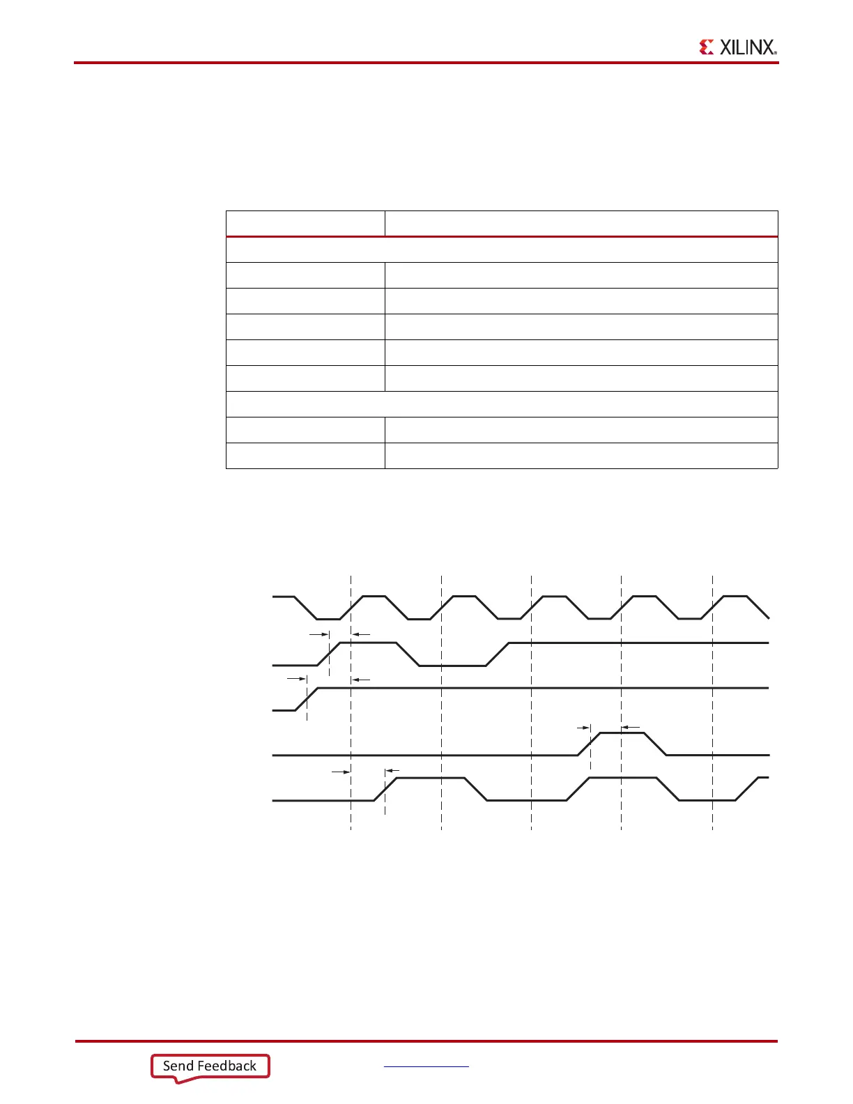
Figure 2-21 illustrates the OLOGIC output register timing.
Clock Event 1
• At time T
OOCECK
before Clock Event 1, the output clock enable signal becomes
valid-high at the OCE input of the output register, enabling the output register for
incoming data.
Table 2-12: OLOGIC Switching Characteristics
Symbol Description
Setup/Hold
T
ODCK
/T
OCKD
D1/D2 pins Setup/Hold with respect to CLK
T
OOCECK
/T
OCKOCE
OCE pin Setup/Hold with respect to CLK
T
OSRCK
/T
OCKSR
S/R pin Setup/Hold with respect to CLK
T
OTCK
/T
OCKT
T1/T2 pins Setup/Hold with respect to CLK
T
OTCECK
/T
OCKTCE
TCE pin Setup/Hold with respect to CLK
Clock to Out
T
OCKQ
CLK to OQ/TQ out
T
RQ
S/R pin to OQ/TQ out
X-Ref Target - Figure 2-2 1
Figure 2-21: OLOGIC Output Register Timing Characteristics
123 45
CLK
D1
OCE
S/R
OQ
T
OCKQ
T
ODCK
T
OOCECK
T
OSRCK
ug471_c2_19_081215