110 www.xilinx.com 7 Series FPGAs SelectIO Resources User Guide
UG471 (v1.10) May 8, 2018
Chapter 2: SelectIO Logic Resources
SAME_EDGE Mode
In the SAME_EDGE mode, the data is presented into the FPGA logic on the same clock
edge. This structure is similar to the Virtex-6 FPGA implementation.
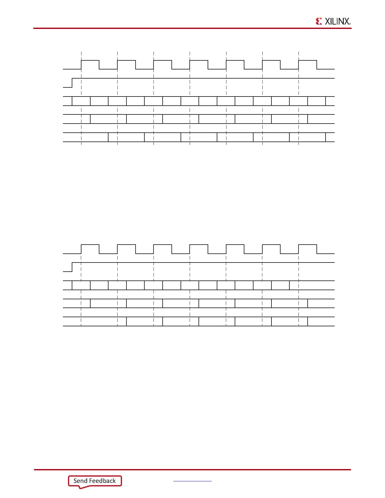
Figure 2-6 shows the timing diagram of the input DDR using SAME_EDGE mode. In the
timing diagram, the output pairs Q1 and Q2 are no longer (0) and (1). Instead, the first pair
presented is pair Q1 (0) and Q2 (don't care), followed by pair (1) and (2) on the next clock
cycle.
SAME_EDGE_PIPELINED Mode
In the SAME_EDGE_PIPELINED mode, the data is presented into the FPGA logic on the
same clock edge.
Unlike the SAME_EDGE mode, the data pair is not separated by one clock cycle. However,
an additional clock latency is required to remove the separated effect of the SAME_EDGE
mode. Figure 2-7 shows the timing diagram of the input DDR using the
SAME_EDGE_PIPELINED mode. The output pairs Q1 and Q2 are presented to the FPGA
logic at the same time.
X-Ref Target - Figure 2-5
Figure 2-5: Input DDR Timing in OPPOSITE_EDGE Mode
ug471_c2_03_090810
C
CE
D
Q1
Q2
D0A D1A D2A
D0A D2A D4A D6A D8A D10A D12A
D1A D3A D5A D7A D9A D11A
D3A
D4A D5A D6A D7A D8A D9A D10A D11A D12A D13A
X-Ref Target - Figure 2-6
Figure 2-6: Input DDR Timing in SAME_EDGE Mode
ug471_c2_04_090810
C
CE
D
Q1
Q2
D1A
D0A D2A D4A D6A D8A D10A
D1A D3A D5A D7A D9A D11A
D3A
D5A D7A D9A D11AD0A D2A D4A D6A D8A D10A
Don't care