166 www.xilinx.com 7 Series FPGAs SelectIO Resources User Guide
UG471 (v1.10) May 8, 2018
Chapter 3: Advanced SelectIO Logic Resources
DATA_WIDTH Attribute
The DATA_WIDTH attribute defines the parallel data input width of the parallel-to-serial
converter. The possible values for this attribute depend on the DATA_RATE_OQ attribute.
When DATA_RATE_OQ is set to SDR, the possible values for the DATA_WIDTH attribute
are 2, 3, 4, 5, 6, 7, and 8. When DATA_RATE_OQ is set to DDR, the possible values for the
DATA_WIDTH attribute are 4, 6, 8, 10, and 14.
When the DATA_WIDTH is set to widths larger than eight, a pair of OSERDESE2 must be
configured into a master-slave configuration. See OSERDESE2 Width Expansion.
SERDES_MODE Attribute
The SERDES_MODE attribute defines whether the OSERDESE2 module is a master or
slave when using width expansion. The possible values are MASTER and SLAVE. The
default value is MASTER. See OSERDESE2 Width Expansion.
TRISTATE_WIDTH Attribute
The TRISTATE_WIDTH attribute defines the parallel 3-state input width of the 3-state
control parallel-to-serial converter. The possible values for this attribute depend on the
DATA_RATE_TQ attribute. When DATA_RATE_TQ is set to SDR or BUF, the
TRISTATE_WIDTH attribute can only be set to 1. When DATA_RATE_TQ is set to DDR,
the possible values for the TRISTATE_WIDTH attribute are 1 and 4.
TRISTATE_WIDTH cannot be set to widths larger than 4. When a DATA_WIDTH is larger
than four, set the TRISTATE_WIDTH to 1.
Table 3-8 shows the valid setting and combinations of using the OSERDESE2.
OSERDESE2 Clocking Methods
The phase relationship of CLK and CLKDIV is important in the parallel-to-serial
conversion process. CLK and CLKDIV are (ideally) phase-aligned within a tolerance.
There are several clocking arrangements within the FPGA to help the design meet the
phase relationship requirements of CLK and CLKDIV. The only valid clocking
arrangements for the OSERDESE2 are:
• CLK driven by BUFIO, CLKDIV driven by BUFR
• CLK and CLKDIV driven by CLKOUT[0:6] of the same MMCM or PLL
When using a MMCM to drive the CLK and CLKDIV of the OSERDESE2 the buffer types
suppling the OSERDESE2 can not be mixed. For example, if CLK is driven by a BUFG,
CLKDIV must be driven by a BUFG as well.
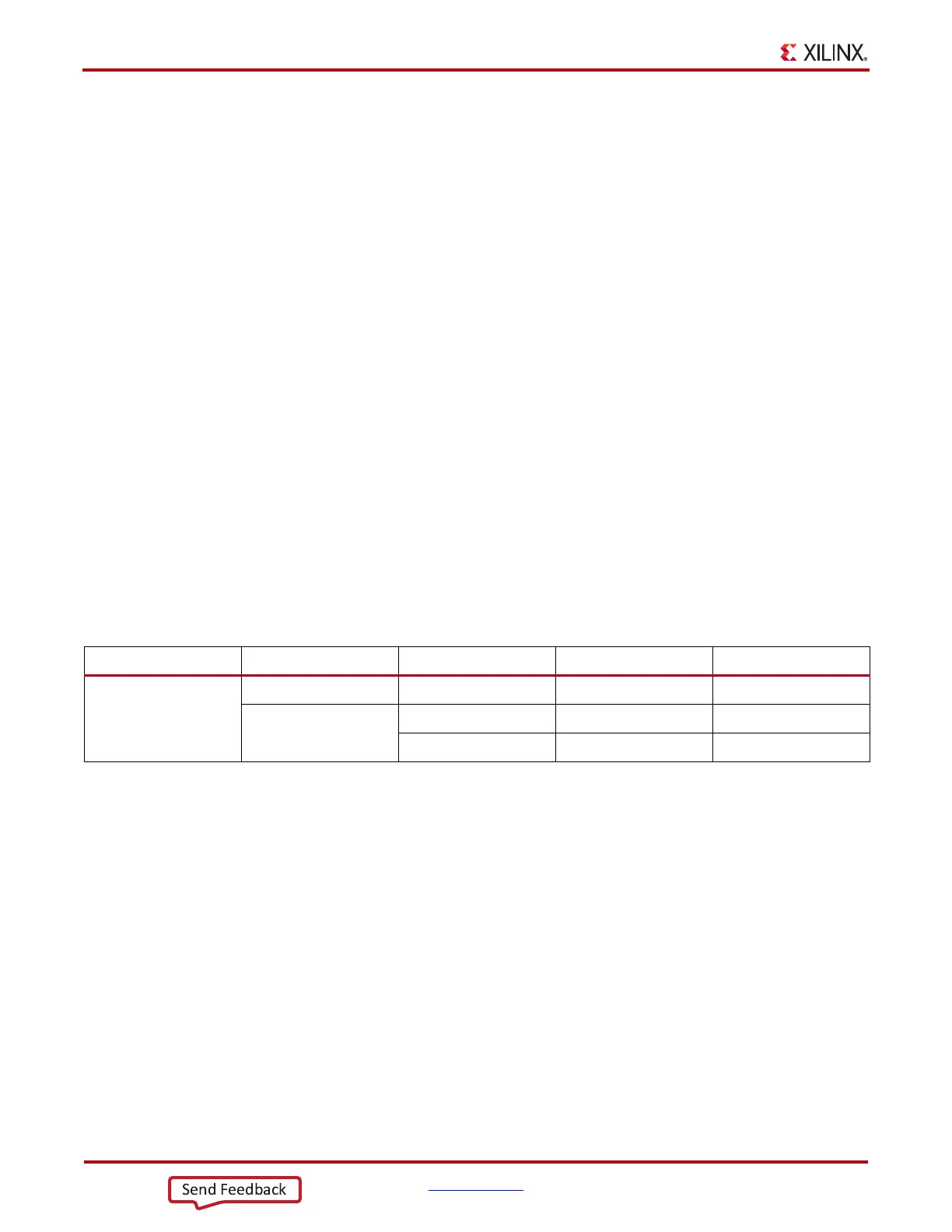
Table 3-8: OSERDESE2 Attribute Combinations
INTERFACE_TYPE DATA_RATE_OQ DATA_RATE_TQ DATA_WIDTH TRISTATE_WIDTH
DEFAULT
SDR SDR 1, 2, 3, 4, 5, 6, 7, 8 1
DDR
DDR 4 4
SDR 2, 6, 8, 10, 14 1