7 Series FPGAs SelectIO Resources User Guide www.xilinx.com 129
UG471 (v1.10) May 8, 2018
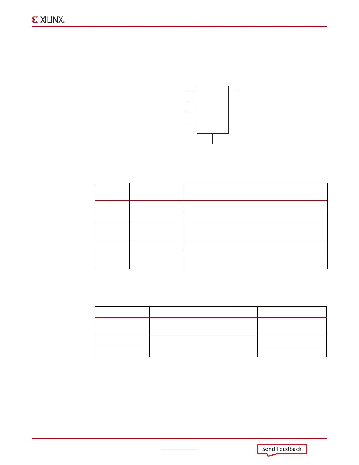
OLOGIC Resources
Output DDR Primitive (ODDR)
Figure 2-20 shows the ODDR primitive block diagram. Set and Reset are not supported at
the same time. Table 2-10 lists the ODDR port signals. Table 2-11 describes the various
attributes available and default values for the ODDR primitive.
ODDR VHDL and Verilog Templates
The Libraries Guide includes templates for instantiation of the ODDR module in VHDL
and Verilog.
X-Ref Target - Figure 2-2 0
Figure 2-20: ODDR Primitive Block Diagram
Table 2-10: ODDR Port Signals
Port
Name
Function Description
Q Data output (DDR) ODDR register output.
C Clock input port The CLK pin represents the clock input pin.
CE Clock enable port CE represents the clock enable pin. When asserted Low,
this port disables the output clock on port Q.
D1 and D2 Data inputs ODDR register inputs.
S/R
(1)
Set/Reset Synchronous/Asynchronous set/reset pin. Set/Reset is
asserted High.
Notes:
1. The ODDR primitive contains both set and reset pins. However only one can be used per ODDR. As a
result, S/R is described instead of separate set and reset pins.
Table 2-11: ODDR Attributes
Attribute Name Description Possible Values
DDR_CLK_EDGE Sets the ODDR mode of operation with
respect to clock edge
OPPOSITE_EDGE
(default), SAME_EDGE
INIT Sets the initial value for Q port 0 (default), 1
SRTYPE Set/Reset type with respect to clock (C) ASYNC, SYNC (default)
ug471_c2_18_022715
C
CE
D1
S/R
Q
D2
ODDR