7 Series FPGAs SelectIO Resources User Guide www.xilinx.com 27
UG471 (v1.10) May 8, 2018
7 Series FPGA DCI—Only available in the HP I/O banks
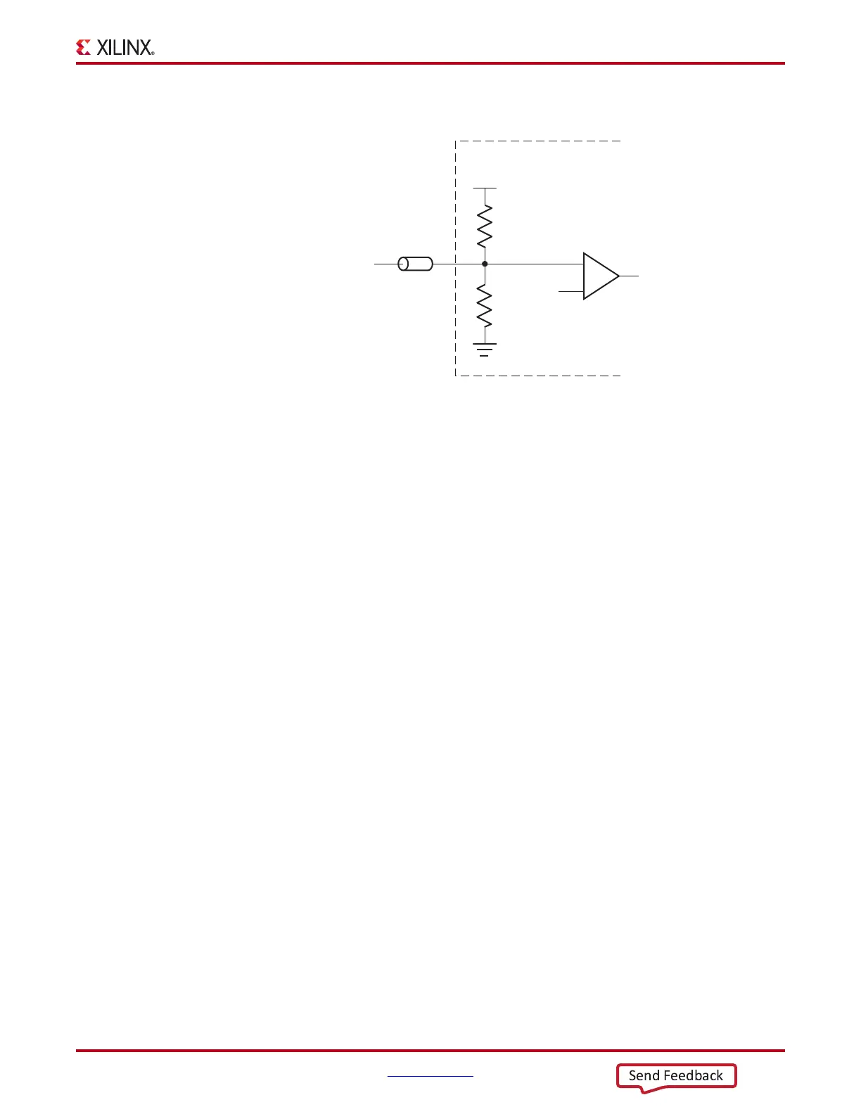
Figure 1-11 illustrates split-termination DCI inside a 7 series device.
VRN/VRP External Resistance Design Migration Guidelines
Previous Xilinx FPGA families featuring DCI used a slightly different circuit for calibrating
the split-termination impedance from the external reference resistors placed on the VRN
and VRP pins. The Virtex-6 FPGA DCI calibrates each leg of the split-termination circuit to
be double the external resistor values. For example, in a Virtex-6 device with a target
parallel termination of 50Ω to V
CCO
/2 requires 50Ω external resistors on the VRN and VRP
pins.
The 7 series FPGAs DCI calibrates each leg of the split termination circuit to be directly
equal to the external resistor values. For example, in a 7 series device with a target parallel
termination of 50Ω to V
CCO
/2 requires 100Ω external resistors on the VRN and VRP pins.
This is particularly important to consider when choosing the VRN and VRP values to be
used in the same I/O bank (or multiple cascaded DCI banks) for both
controlled-impedance DCI and split-termination DCI standards.
In a Virtex-6 FPGA design with a 50Ω target controlled impedance driver for an LVDCI_18
output and a 50Ω target split-termination receiver for an HSTL_I_DCI_18 input, can be
implemented using 50Ω external resistors on the VRN and VRP pins. To migrate this same
design to a 7 series FPGA would not change the HSTL_I_DCI_18 I/O standard; however,
the external resistors must change to 100Ω and the controlled impedance driver changes to
an LVDCI_DIV2_18 output. This example outcome is equivalent; however both resistor
values and I/O standard changes are required. A power rating of 0.05W or higher can be
safely used for the VRN and VRP external resistors.
X-Ref Target - Figure 1-1 1
Figure 1-11: Input Termination to V
CCO
/2 Using Split-Termination DCI
(External Resistors on VRN, VRP = 2R)
2R
2R
UG471_c1_13_011811
V
CCO
V
REF
IOB
Z
0
7 Series FPGA HP Bank DCI