EasyManua.ls Logo

Xilinx SelectIO 7 Series User Manual

Xilinx SelectIO 7 Series
188 pages
To Next Page IconTo Next Page
To Previous Page IconTo Previous Page
Page #45 background imageLoading...
Page #45 background image
7 Series FPGAs SelectIO Resources User Guide www.xilinx.com 45
UG471 (v1.10) May 8, 2018
7 Series FPGA SelectIO Primitives
split-termination feature. See Uncalibrated Split Termination in High-Range I/O Banks
(IN_TERM) for more details on this feature.
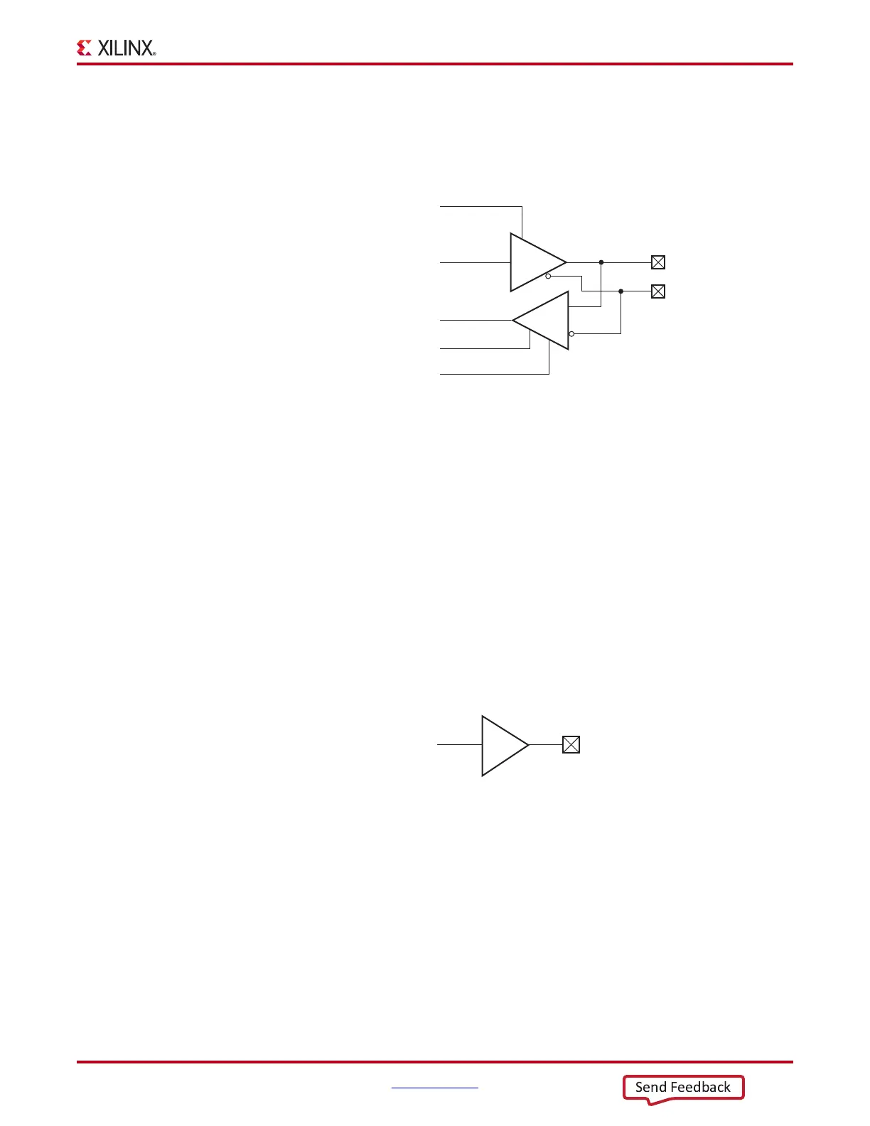
The IOBUFDS_INTERMDISABLE primitive can disable the input buffer and force the O
output to the fabric to a logic High when the USE_IBUFDISABLE attribute is set to TRUE
and the IBUFDISABLE signal is asserted High. If USE_IBUFDISABLE is set to FALSE, this
input is ignored and should be tied to ground. If the I/O is using the optional uncalibrated
split-termination feature (IN_TERM), those termination legs are disabled whenever the
driver is active (T is low). This primitive further allows the termination legs to be disabled
whenever the INTERMDISABLE signal is asserted High. These features can be combined
to reduce power whenever the input is idle for a period of time.
OBUF
An output buffer (OBUF) must be used to drive signals from 7 series devices to external
output pads. A generic 7 series FPGA OBUF primitive is shown in Figure 1-33.
OBUFDS
Figure 1-34 shows the differential output buffer primitive.
X-Ref Target - Figure 1-3 2
Figure 1-32: Differential Bidirectional Buffer With Input Buffer Disable and
IN_TERM Disable (IOBUFDS_INTERMDISABLE)
IOBUFDS_INTERMDISABLE
IBUFDISABLE
INTERMDISABLE
T
I
O
IO
IOB
UG471_c1_68_021214
X-Ref Target - Figure 1-33
Figure 1-33: Output Buffer Primitive (OBUF)
ug471_c1_18_011811
OBUF
O (Output)
to device pad
I (Input)
From FPGA
Send Feedback

Table of Contents

Question and Answer IconNeed help?

Do you have a question about the Xilinx SelectIO 7 Series and is the answer not in the manual?

Xilinx SelectIO 7 Series Specifications

General IconGeneral
FPGA Family7 Series
Programmable Slew RateYes
Programmable Output StrengthYes
Hot Swap CapabilityYes
I/O Standard SupportLVCMOS, LVTTL, HSTL, SSTL
Programmable TerminationYes
ConfigurationJTAG, SPI
Input Delay ElementsYes
Output Delay ElementsYes
Differential TerminationYes
Compatible SeriesVirtex-7, Kintex-7, Artix-7
Maximum I/O PinsUp to 1200+ (device dependent)

Summary

Preface

About This Guide

Provides an overview of the document's scope and content.

Guide Contents

Lists the chapters covered in the user guide.

Additional Resources

Points to further documentation and support resources.

Chapter 1: SelectIO Resources

I/O Tile Overview

Describes the basic structure and components of SelectIO I/O tiles.

SelectIO Resources General Guidelines

Summarizes general design rules for using SelectIO resources.

7 Series FPGA DCI—Only available in the HP I/O banks

Explains Digitally Controlled Impedance (DCI) and its availability in HP I/O banks.

Uncalibrated Split Termination in High-Range I/O Banks (IN_TERM)

Details the uncalibrated split termination feature in HR I/O banks.

7 Series FPGA SelectIO Primitives

Introduces the various I/O buffer primitives available for SelectIO resources.

7 Series FPGA SelectIO Attributes/Constraints

Covers attributes and constraints for configuring SelectIO I/O features.

Supported I/O Standards and Terminations

Provides an overview of supported I/O standards and their termination options.

Rules for Combining I/O Standards in the Same Bank

Outlines rules for mixing different I/O standards within the same I/O bank.

Simultaneous Switching Outputs

Discusses analysis and mitigation of noise from simultaneous switching outputs (SSOs).

Pin Planning to Mitigate SSO Sensitivity

Offers guidance on pin planning to reduce sensitivity to SSO noise.

Chapter 2: SelectIO Logic Resources

ILOGIC Resources

Describes the input logic blocks (ILOGIC) for data capture and processing.

Input DDR Overview (IDDR)

Explains the Double Data Rate (DDR) input registers and their operational modes.

Input Delay Resources (IDELAY)

Details the programmable delay primitive (IDELAYE2) for fine-tuning input timing.

IDELAY Attributes

Lists and describes the attributes for configuring the IDELAY primitive.

IDELAY Modes

Explains the different operational modes for the IDELAY primitive.

IDELAYCTRL

Describes the IDELAYCTRL module for calibrating delay taps.

OLOGIC Resources

Describes the output logic blocks (OLOGIC) for data output and 3-state control.

Output DDR Overview (ODDR)

Explains the Double Data Rate (DDR) output registers and their operational modes.

Output Delay Resources (ODELAY)—Not Available in HR Banks

Details the programmable delay primitive (ODELAYE2) for output timing adjustment.

ODELAY Attributes

Lists and describes the attributes for configuring the ODELAY primitive.

ODELAY Modes

Explains the different operational modes for the ODELAY primitive.

Chapter 3: Advanced SelectIO Logic Resources

Input Serial-to-Parallel Logic Resources (ISERDESE2)

Introduces the ISERDESE2 for high-speed serial-to-parallel conversion.

ISERDESE2 Primitive (ISERDESE2)

Describes the ISERDESE2 primitive and its ports.

ISERDESE2 Attributes

Lists and describes the attributes for configuring the ISERDESE2.

ISERDESE2 Clocking Methods

Explains clocking arrangements for ISERDESE2 in different interface types.

ISERDESE2 Width Expansion

Details how to expand ISERDESE2 modules for wider parallel interfaces.

Bitslip Timing Model and Parameters

Explains the timing and operation of the Bitslip submodule.

Output Parallel-to-Serial Logic Resources (OSERDESE2)

Introduces the OSERDESE2 for high-speed parallel-to-serial conversion.

OSERDESE2 Primitive

Describes the OSERDESE2 primitive and its ports.

OSERDESE2 Attributes

Lists and describes the attributes for configuring the OSERDESE2.

OSERDESE2 Width Expansion

Details how to expand OSERDESE2 modules for wider parallel interfaces.

OSERDESE2 Latencies

Summarizes the latency values for OSERDESE2 based on data rate and width.

Timing Characteristics of 2:1 SDR Serialization

Illustrates the timing for 2:1 SDR serialization.

Timing Characteristics of 8:1 DDR Serialization

Illustrates the timing for 8:1 DDR serialization.

Timing Characteristics of 4:1 DDR 3-State Controller Serialization

Illustrates the timing for 4:1 DDR 3-state serialization.

IO_FIFO Overview

Provides an overview of the IO_FIFO resources for I/O data transfer.

IN_FIFO

Describes the IN_FIFO primitive and its modes of operation.

OUT_FIFO

Describes the OUT_FIFO primitive and its modes of operation.

Appendix A: Termination Options for SSO Noise Analysis

Default Terminations for SSN Noise Analysis by I/O Standard

Lists default off-chip termination options for SSN analysis.

Related product manuals