EasyManua.ls Logo

Xilinx SelectIO 7 Series User Manual

Xilinx SelectIO 7 Series
188 pages
To Next Page IconTo Next Page
To Previous Page IconTo Previous Page
Page #127 background imageLoading...
Page #127 background image
7 Series FPGAs SelectIO Resources User Guide www.xilinx.com 127
UG471 (v1.10) May 8, 2018
OLOGIC Resources
This section of the documentation discusses the various features available using the
OLOGIC resources.
Combinatorial Output Data and 3-State Control Path
The combinatorial output paths create a direct connection from the FPGA logic to the
output driver or output driver control. These paths are used automatically by software
when:
1. There is direct (unregistered) connection from logic resources in the FPGA logic to the
output data or 3-state control.
2. The
pack I/O register/latches into IOBs software map directive is set to OFF.
Output DDR Overview (ODDR)
7 series devices have dedicated registers in the OLOGIC to implement output DDR
registers. This feature is accessed when instantiating the ODDR primitive. DDR
multiplexing is automatic when using OLOGIC. No manual control of the mux-select is
needed. This control is generated from the clock.
There is only one clock input to the ODDR primitive. Falling edge data is clocked by a
locally inverted version of the input clock. All clocks feeding into the I/O tile are fully
multiplexed, i.e., there is no clock sharing between the ILOGIC or the OLOGIC blocks. The
ODDR primitive supports the following modes of operation:
OPPOSITE_EDGE mode
SAME_EDGE mode
The SAME_EDGE mode is the same as for the Virtex-6 architecture. This mode allows
designers to present both data inputs to the ODDR primitive on the rising-edge of the
ODDR clock, saving CLB and clock resources, and increasing performance. This mode is
implemented using the DDR_CLK_EDGE attribute. It is supported for 3-state control as
well. The following sections describe each of the modes in detail.
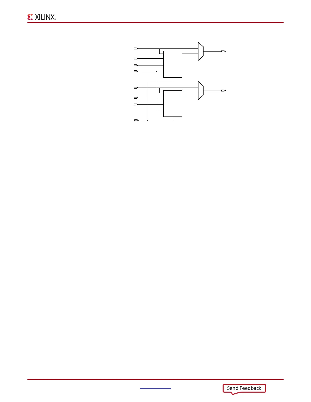
X-Ref Target - Figure 2-1 7
Figure 2-17: OLOGIC Block Diagram
D1
D2
T1
T2
TCE
CLK
S/R
Q
TQ
CE
CK
S/R
ug471_c2_15_022715
D1
D2
D1
D2
OCE
Q
OQ
CE
CK
S/R
Send Feedback

Table of Contents

Question and Answer IconNeed help?

Do you have a question about the Xilinx SelectIO 7 Series and is the answer not in the manual?

Xilinx SelectIO 7 Series Specifications

General IconGeneral
FPGA Family7 Series
Programmable Slew RateYes
Programmable Output StrengthYes
Hot Swap CapabilityYes
I/O Standard SupportLVCMOS, LVTTL, HSTL, SSTL
Programmable TerminationYes
ConfigurationJTAG, SPI
Input Delay ElementsYes
Output Delay ElementsYes
Differential TerminationYes
Compatible SeriesVirtex-7, Kintex-7, Artix-7
Maximum I/O PinsUp to 1200+ (device dependent)

Summary

Preface

About This Guide

Provides an overview of the document's scope and content.

Guide Contents

Lists the chapters covered in the user guide.

Additional Resources

Points to further documentation and support resources.

Chapter 1: SelectIO Resources

I/O Tile Overview

Describes the basic structure and components of SelectIO I/O tiles.

SelectIO Resources General Guidelines

Summarizes general design rules for using SelectIO resources.

7 Series FPGA DCI—Only available in the HP I/O banks

Explains Digitally Controlled Impedance (DCI) and its availability in HP I/O banks.

Uncalibrated Split Termination in High-Range I/O Banks (IN_TERM)

Details the uncalibrated split termination feature in HR I/O banks.

7 Series FPGA SelectIO Primitives

Introduces the various I/O buffer primitives available for SelectIO resources.

7 Series FPGA SelectIO Attributes/Constraints

Covers attributes and constraints for configuring SelectIO I/O features.

Supported I/O Standards and Terminations

Provides an overview of supported I/O standards and their termination options.

Rules for Combining I/O Standards in the Same Bank

Outlines rules for mixing different I/O standards within the same I/O bank.

Simultaneous Switching Outputs

Discusses analysis and mitigation of noise from simultaneous switching outputs (SSOs).

Pin Planning to Mitigate SSO Sensitivity

Offers guidance on pin planning to reduce sensitivity to SSO noise.

Chapter 2: SelectIO Logic Resources

ILOGIC Resources

Describes the input logic blocks (ILOGIC) for data capture and processing.

Input DDR Overview (IDDR)

Explains the Double Data Rate (DDR) input registers and their operational modes.

Input Delay Resources (IDELAY)

Details the programmable delay primitive (IDELAYE2) for fine-tuning input timing.

IDELAY Attributes

Lists and describes the attributes for configuring the IDELAY primitive.

IDELAY Modes

Explains the different operational modes for the IDELAY primitive.

IDELAYCTRL

Describes the IDELAYCTRL module for calibrating delay taps.

OLOGIC Resources

Describes the output logic blocks (OLOGIC) for data output and 3-state control.

Output DDR Overview (ODDR)

Explains the Double Data Rate (DDR) output registers and their operational modes.

Output Delay Resources (ODELAY)—Not Available in HR Banks

Details the programmable delay primitive (ODELAYE2) for output timing adjustment.

ODELAY Attributes

Lists and describes the attributes for configuring the ODELAY primitive.

ODELAY Modes

Explains the different operational modes for the ODELAY primitive.

Chapter 3: Advanced SelectIO Logic Resources

Input Serial-to-Parallel Logic Resources (ISERDESE2)

Introduces the ISERDESE2 for high-speed serial-to-parallel conversion.

ISERDESE2 Primitive (ISERDESE2)

Describes the ISERDESE2 primitive and its ports.

ISERDESE2 Attributes

Lists and describes the attributes for configuring the ISERDESE2.

ISERDESE2 Clocking Methods

Explains clocking arrangements for ISERDESE2 in different interface types.

ISERDESE2 Width Expansion

Details how to expand ISERDESE2 modules for wider parallel interfaces.

Bitslip Timing Model and Parameters

Explains the timing and operation of the Bitslip submodule.

Output Parallel-to-Serial Logic Resources (OSERDESE2)

Introduces the OSERDESE2 for high-speed parallel-to-serial conversion.

OSERDESE2 Primitive

Describes the OSERDESE2 primitive and its ports.

OSERDESE2 Attributes

Lists and describes the attributes for configuring the OSERDESE2.

OSERDESE2 Width Expansion

Details how to expand OSERDESE2 modules for wider parallel interfaces.

OSERDESE2 Latencies

Summarizes the latency values for OSERDESE2 based on data rate and width.

Timing Characteristics of 2:1 SDR Serialization

Illustrates the timing for 2:1 SDR serialization.

Timing Characteristics of 8:1 DDR Serialization

Illustrates the timing for 8:1 DDR serialization.

Timing Characteristics of 4:1 DDR 3-State Controller Serialization

Illustrates the timing for 4:1 DDR 3-state serialization.

IO_FIFO Overview

Provides an overview of the IO_FIFO resources for I/O data transfer.

IN_FIFO

Describes the IN_FIFO primitive and its modes of operation.

OUT_FIFO

Describes the OUT_FIFO primitive and its modes of operation.

Appendix A: Termination Options for SSO Noise Analysis

Default Terminations for SSN Noise Analysis by I/O Standard

Lists default off-chip termination options for SSN analysis.

Related product manuals