174 www.xilinx.com 7 Series FPGAs SelectIO Resources User Guide
UG471 (v1.10) May 8, 2018
Chapter 3: Advanced SelectIO Logic Resources
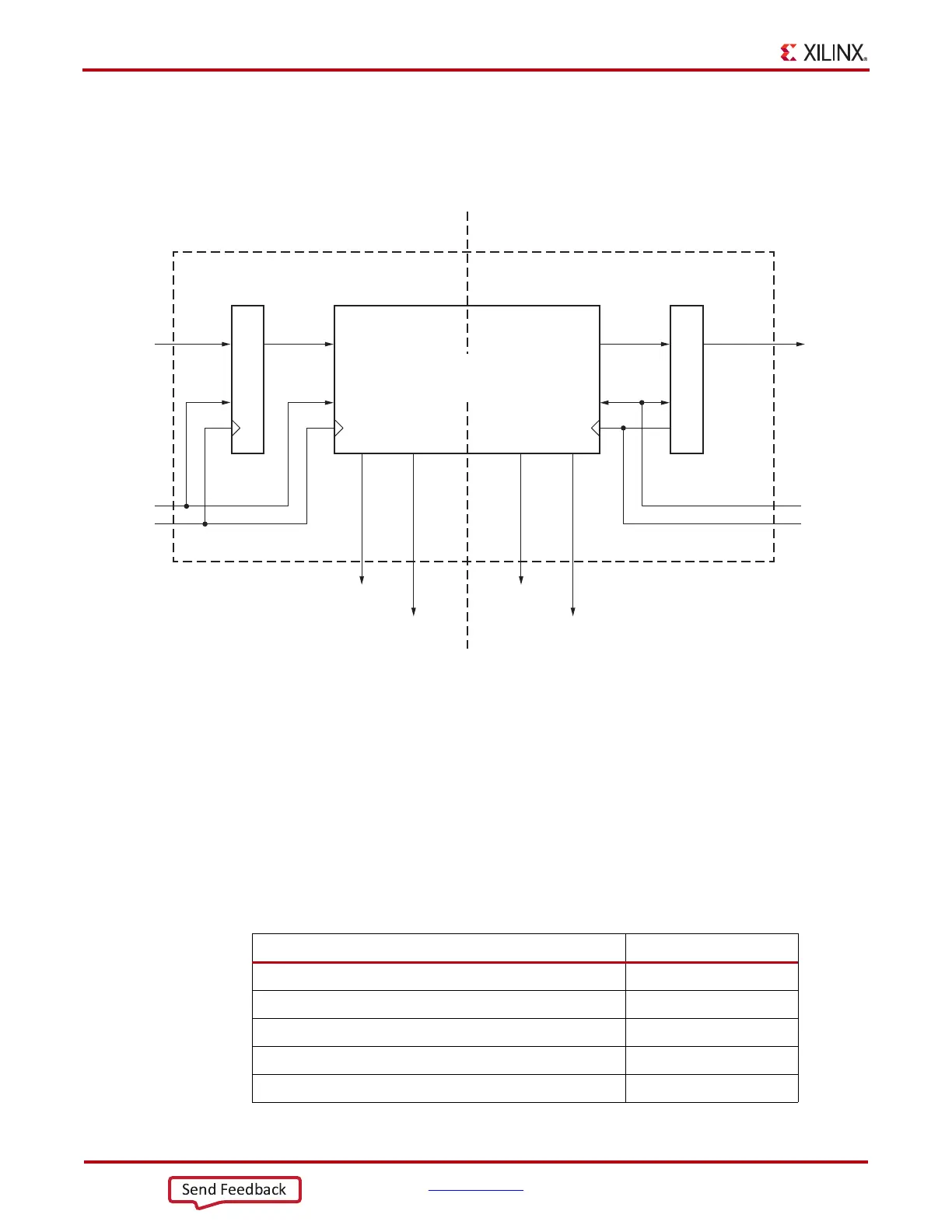
The IO_FIFOs have an input register, a 7-entry deep FIFO core, and an output register (see
Figure 3-19). The input and output registers are an integral part of the IO_FIFO and
provide the eighth storage location for the full IO_FIFO. The registers, FIFO core, and
control signals are treated as a single atomic unit.
IN_FIFO
The IN_FIFO is physically aligned to an I/O byte group for optimized performance. The
8-entry deep IN_FIFO supports data transfer using two modes of operation:
• 4 x 4 mode – This mode configures the FIFO to have 12 4-bit wide data inputs (D) and
12 4-bit wide data outputs (Q). The D0[3:0] – D9[3:0] ports map to the Q0[3:0] –
Q9[3:0] ports. D5[7:4] and D6[7:4] are the two extra data input ports D10[3:0] and
D11[3:0] and map to the Q5[7:4] and Q6[7:4] extra output ports Q10[3:0] and Q11[3:0].
The other Qn[7:4] ports are not used. Table 3-13 shows the 4 x 4 mode mapping in
detail.
X-Ref Target - Figure 3-19
Figure 3-19: IO_FIFO Architecture: Top-Level View
Write Clock Domain
8 Clock Cycles
Read Clock Domain
8 Clock Cycles
Q
D
EN
FULL EMPTY
ALMOSTFULL ALMOSTEMPTY
EN
WREN
WRCLK
RDEN
RDCLK
FIFO Core
7 Entries Deep
Register Register
UG471_c3_19_111011
D Q
Table 3-13: IN_FIFO Input to Output Data Mapping in 4 x 4 Mode
Mapping Not Used
D0[3:0] → Q0[3:0] Q0[7:4]
D1[3:0] → Q1[3:0] Q1[7:4]
D2[3:0] → Q2[3:0] Q2[7:4]
D3[3:0] → Q3[3:0] Q3[7:4]
D4[3:0] → Q4[3:0] Q4[7:4]