46 www.xilinx.com 7 Series FPGAs SelectIO Resources User Guide
UG471 (v1.10) May 8, 2018
Chapter 1: SelectIO Resources
OBUFT
The generic 3-state output buffer OBUFT, shown in Figure 1-35, typically implements
3-state outputs or bidirectional I/O.
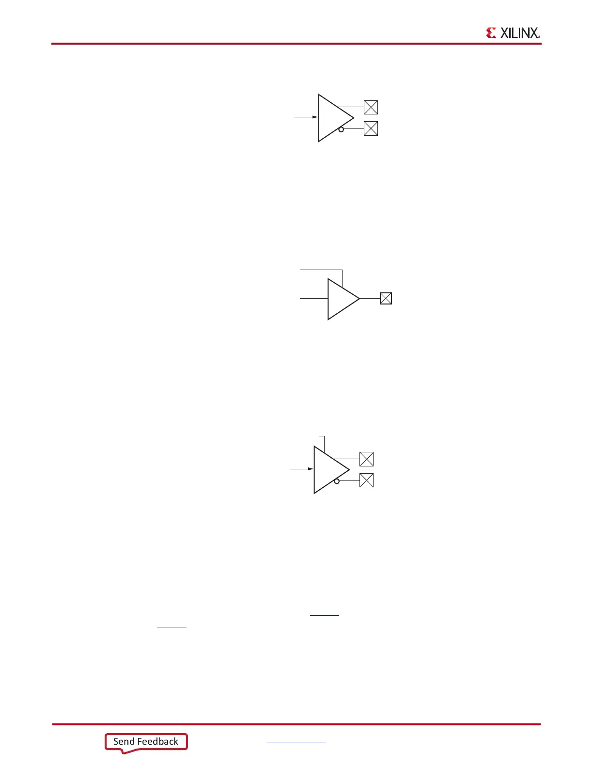
OBUFTDS
Figure 1-36 shows the differential 3-state output buffer primitive.
7 Series FPGA SelectIO Attributes/Constraints
Access to some 7 series FPGA I/O resource features (e.g., location constraints, input delay,
output drive strength, and slew rate) is available through the attributes/constraints
associated with these features. For more information about implementing these constraints
and attributes as well as others, see UG625
: Constraints Guide (for the ISE tools) or
UG912
: Vivado Design Suite Properties Reference Guide.
DCI_CASCADE Constraint
The DCI_CASCADE constraint identifies a DCI master bank and its corresponding slave
banks. See DCI Cascading, page 22 for more information.
X-Ref Target - Figure 1-3 4
Figure 1-34: Differential Output Buffer Primitive (OBUFDS)
ug471_c1_22_041112
+
–
OB
O
I
OBUFDS
Input from
FPGA
Output to
Device Pads
X-Ref Target - Figure 1-3 5
Figure 1-35: 3-State Output Buffer Primitive (OBUFT)
ug471_c1_19_011811
OBUFT
O (Output)
to device pad
I (Input)
From FPGA
T
3-state input
X-Ref Target - Figure 1-3 6
Figure 1-36: Differential 3-state Output Buffer Primitive (OBUFTDS)
ug471_c1_23_041112
+
–
OB
O
I
T
OBUFTDS
Input from
FPGA
3-state Input
Output to
Device Pads