7 Series FPGAs SelectIO Resources User Guide www.xilinx.com 113
UG471 (v1.10) May 8, 2018
ILOGIC Resources
ILOGIC Timing Models
This section describes the timing associated with the various resources within the ILOGIC
block.
ILOGIC Timing Characteristics
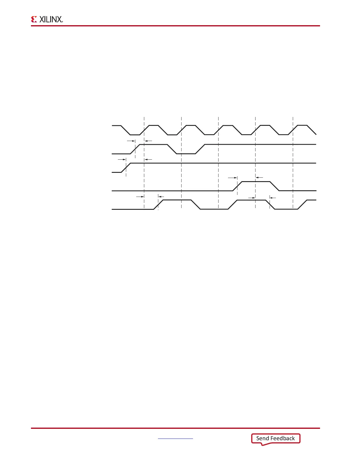
Figure 2-9 illustrates ILOGIC register timing. When IDELAY is used, T
IDOCK
is replaced by
T
IDOCKD
.
Clock Event 1
• At time T
ICE1CK
before Clock Event 1, the input clock enable signal becomes
valid-high at the CE1 input of the input register, enabling the input register for
incoming data.
• At time T
IDOCK
before Clock Event 1, the input signal becomes valid-high at the D
input of the input register and is reflected on the Q1 output of the input register at
time T
ICKQ
after Clock Event 1.
Clock Event 4
•At time T
ISRCK
before Clock Event 4, the S/R signal (configured as synchronous reset
in this case) becomes valid-high resetting the input register and reflected at the Q1
output of the IOB at time T
ICKQ
after Clock Event 4.
ILOGIC Timing Characteristics, DDR
Figure 2-10 illustrates the ILOGIC in IDDR mode timing characteristics. When IDELAY is
used, T
IDOCK
is replaced by T
IDOCKD
. The example shown uses IDDR in
OPPOSITE_EDGE mode. For other modes, add the appropriate latencies as shown in
Figure 2-7, page 111.
X-Ref Target - Figure 2-9
Figure 2-9: ILOGIC Input Register Timing Characteristics
123 45
CLK
D
CE1
S/R
Q1
T
ICKQ
T
ICKQ
T
IDOCK
T
ICE1CK
T
ISRCK
ug471_c2_07_081215