7 Series FPGAs SelectIO Resources User Guide www.xilinx.com 135
UG471 (v1.10) May 8, 2018
Output Delay Resources (ODELAY)—Not Available in HR Banks
ODELAY Ports
Data Input from the FPGA OLOGICE2/OSERDESE2 - ODATAIN
The ODATAIN input is driven by OLOGICE2/OSERDESE2. The ODATAIN drives the
DATAOUT port which is connected to an IOB with a delay set by the ODELAY_VALUE.
Clock Input from Clock Buffer - CLKIN
The CLKIN input is driven from clock buffers (BUFIO, BUFG or BUFR). This clock is then
delayed by a value set to ODELAY_VALUE and output though the DATAOUT and output
buffer (OBUFT or OBUFTDS). When an IOBUF is used, the delayed clock can be routed
back to the FPGA logic.
Caution!
Be aware that a package pin of the FPGA is used when using an IOBUF to route a
clock back into the FPGA.
Data Output - DATAOUT
Delayed data from one of the two data input ports. DATAOUT connects to the IOB.
Clock Input - C
All control inputs to ODELAYE2 primitive (LD, CE, and INC) are synchronous to the clock
input (C). A clock must be connected to this port when ODELAY is configured in
VARIABLE, VAR_LOAD, or VAR_LOAD_PIPE mode. C can be locally inverted, and must
be supplied by a global or regional clock buffer. This clock must be connected to the same
clock as used in the SelectIO logic resources. For example, when using the OSERDESE2,
C is connected to the same clock as CLKDIV. If the IDELAYE2 primitive is used in the same
I/O bank as the ODELAYE2 primitive, C must use the same clock net for both primitives.
Module Load - LD
When in VARIABLE mode, the ODELAY load port, LD, loads the delay primitive to a
value set by the ODELAY_VALUE attribute. If these attributes are not specified, a value of
zero is assumed. The LD signal is an active-High signal and is synchronous to the input
clock signal (C).
When in VAR_LOAD mode, the ODELAY load port, LD, loads the delay primitive to a
value set by the CNTVALUEIN. The value present at CNTVALUEIN[4:0] will be the new
tap value. As a result of this functionality the ODELAY_VALUE attribute is ignored.
When in VAR_LOAD_PIPE mode, the IDELAY load port, LD, loads the value currently in
the pipeline register. The value present in the pipeline register will be the new tap value.
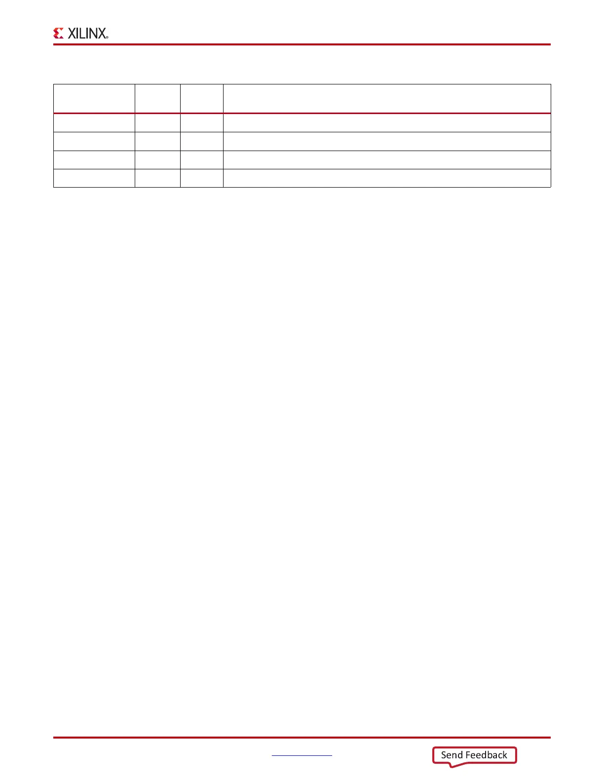
ODATAIN Input 1 Data input for ODELAY from the OLOGICE2/OSERDESE2.
LDPIPEEN Input 1
Enables the pipeline register to load data from CNTVALUEIN.
DATAOUT Output 1 Delayed data from one of two data input ports (ODATAIN and CLKIN).
CNTVALUEOUT Output 5 Current delay value going to FPGA logic for monitoring tap value.
Table 2-13: ODELAYE2 Primitive Ports (Cont’d)
Port
Name
Direction Width Function