72 www.xilinx.com 7 Series FPGAs SelectIO Resources User Guide
UG471 (v1.10) May 8, 2018
Chapter 1: SelectIO Resources
HSTL_II_T_DCI (1.5V or 1.8V) Split-Thevenin Termination (3-state)
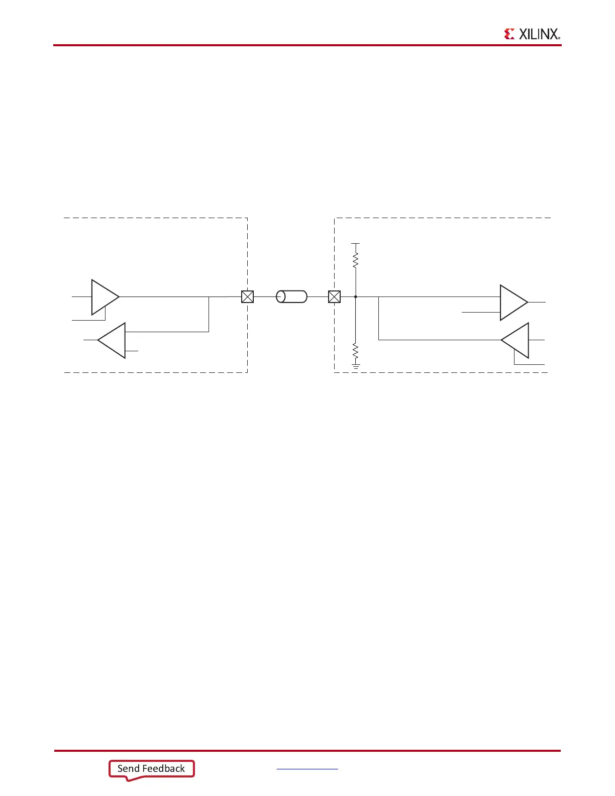
Figure 1-55 shows a sample circuit illustrating a termination technique for HSTL_II_T_DCI
(1.5V) and HSTL_II_T_DCI_18 (1.8V) with on-chip split-thevenin termination. In this
bidirectional case, when 3-stated, the termination is invoked on the receiver and not on the
driver. In a specific circuit, all drivers and receivers must be at the same voltage level
(either 1.5V or 1.8V); they are not interchangeable. Only HP I/O banks support the T_DCI
standards. The internal split-termination resistors are only present when the output
buffers are 3-stated.
X-Ref Target - Figure 1-55
Figure 1-55: HSTL_II_T_DCI (1.5V) and HSTL_II_T_DCI_18 (1.8V) Split-Thevenin Termination (3-state)
ug471_c1_45_021214
Z
0
IOB
IOB
1
0
HSTL_II_T_DCI
HSTL_II_T_DCI_18
HSTL_II_T_DCI
HSTL_II_T_DCI_18
V
CCO
= 1.5V for HSTL_II_T_DCI
1.8V for HSTL_II_T_DCI_18
R
VRN
= 2Z
0
= 100Ω
R
VRP
= 2Z
0
= 100Ω
V
REF
=
0.75V for HSTL_II_T_DCI
0.9V for HSTL_II_T_DCI_18
V
REF
=
0.75V for HSTL_II_T_DCI
0.9V for HSTL_II_T_DCI_18
+
–
DCI
Not 3-stated
(T pin logic Low)
3-stated
(T pin logic High)