263
ABOV Semiconductor Co., Ltd.
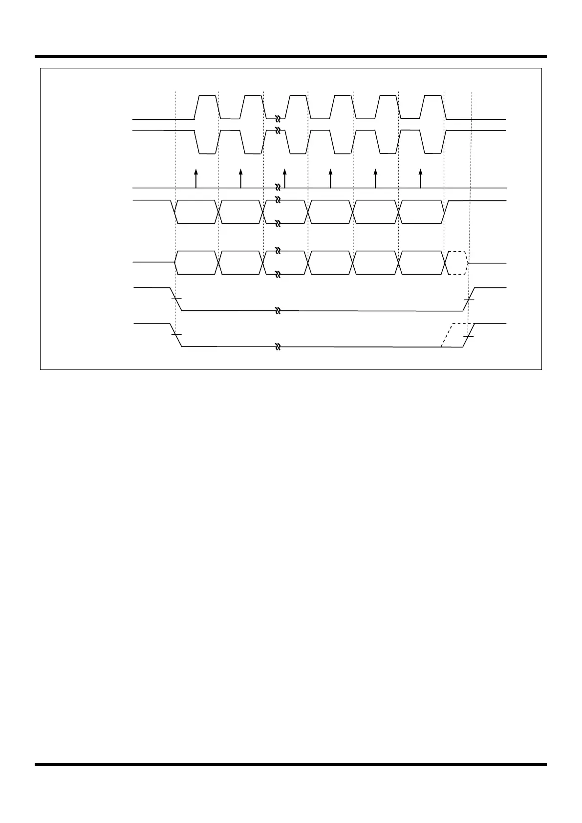
Figure 11.69 USI0/1 SPI Clock Formats when CPHAn=0 (where n = 0 and 1)
When CPHAn=0, the slave begins to drive its MISOn output with the first data bit value when SSn goes to active low.
The first SCKn edge causes both the master and the slave to sample the data bit value on their MISOn and MOSIn
inputs, respectively. At the second SCKn edge, the USI0/1 shifts the second data bit value out to the MOSIn and
MISOn outputs of the master and slave, respectively. Unlike the case of CPHAn=1, when CPHAn=0, the slave’s SSn
input must go to its inactive high level between transfers. This is because the slave can prepare the first data bit when
it detects falling edge of SSn input.