264
ABOV Semiconductor Co., Ltd.
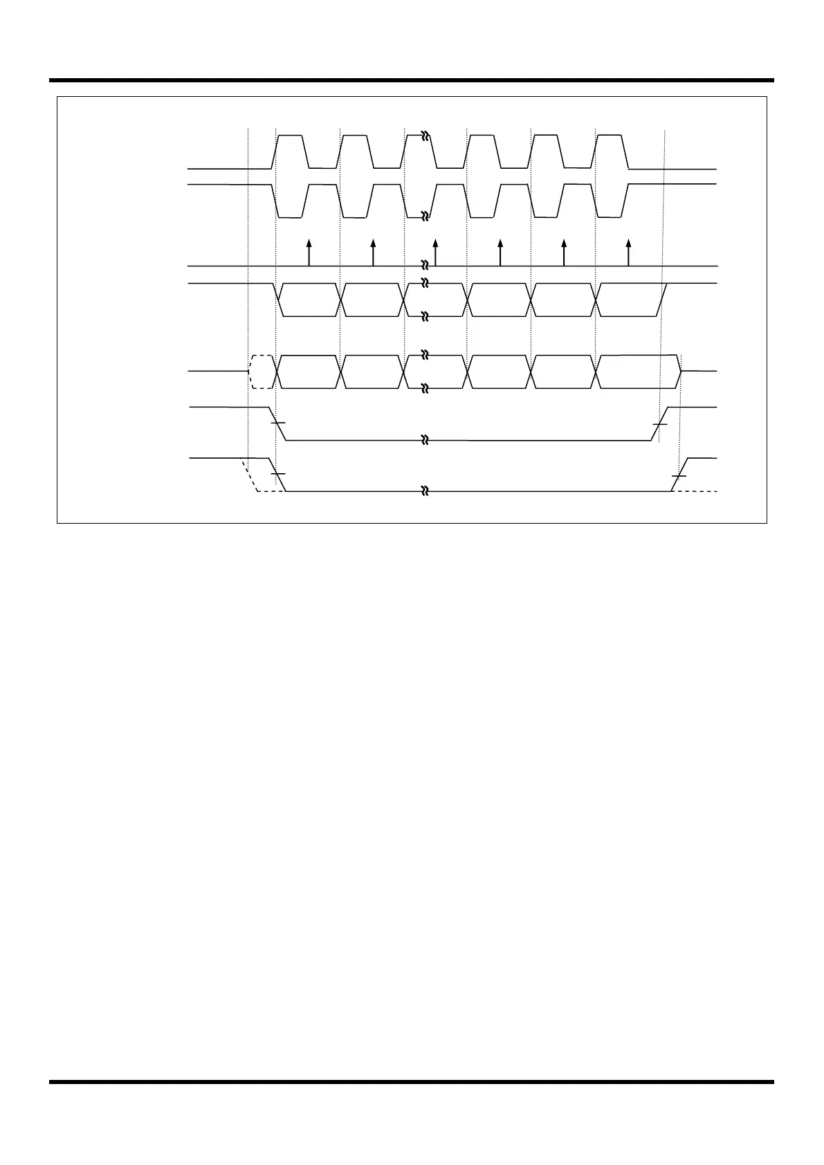
Figure 11.70 USI0/1 SPI Clock Formats when CPHAn=1 (where n = 0 and 1)
When CPHAn=1, the slave begins to drive its MISOn output when SSn goes active low, but the data is not defined
until the first SCKn edge. The first SCKn edge shifts the first bit of data from the shifter onto the MOSIn output of the
master and the MISOn output of the slave. The next SCKn edge causes both the master and slave to sample the data
bit value on their MISOn and MOSIn inputs, respectively. At the third SCKn edge, the USI0/1 shifts the second data bit
value out to the MOSIn and MISOn output of the master and slave respectively. When CPHAn=1, the slave’s SSn
input is not required to go to its inactive high level between transfers.
Because the SPI logic reuses the USI0/1 resources, SPI mode of operation is similar to that of synchronous or
asynchronous operation. An SPI transfer is initiated by checking for the USI0/1 Data Register Empty flag (DREn=1)
and then writing a byte of data to the USInDR Register. In master mode of operation, even if transmission is not
enabled (TXEn=0), writing data to the USInDR register is necessary because the clock SCKn is generated from
transmitter block.