Host Bridge/DRAM Controller Registers (D0:F0)
R
Intel
®
82925X/82925XE MCH Datasheet 47
Address
Offset
Register
Symbol
Register Name
Default
Value
Access
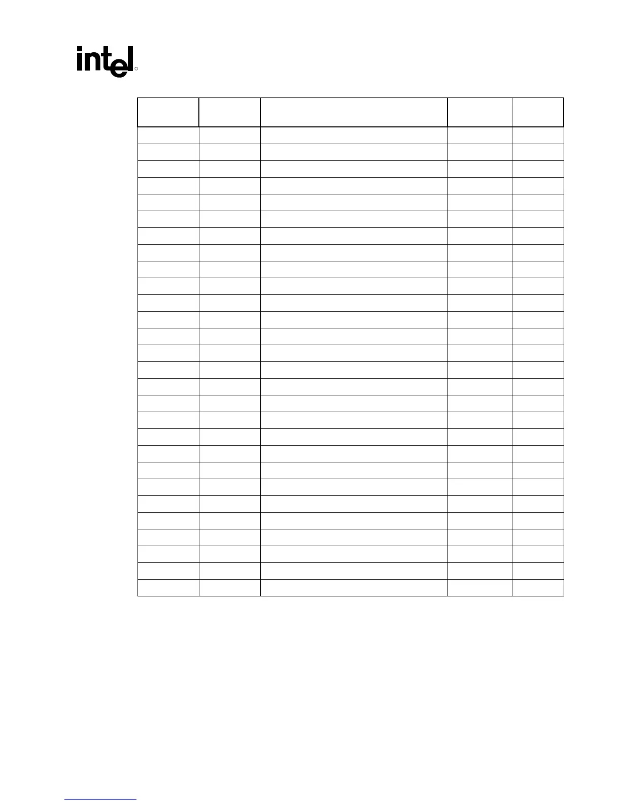
109h C0DRA2 Channel A DRAM Rank 2,3 Attribute 00h R/W
10Ah–10Bh — Reserved — —
10Ch C0DCLKDIS Channel A DRAM Clock Disable 00h R/W
10Dh — Reserved — —
10E–10F C0BNKARC Channel A DRAM Bank Architecture 0000h R/W
110h–113h — Reserved — —
114h–117h C0DRT1 Channel A DRAM Timing Register 900122h R/W
118h–11Fh — Reserved — —
120h–123h C0DRC0 Channel A DRAM Controller Mode 0 00000000h R/W, RO
124h–17Fh — Reserved — —
180h C1DRB0 Channel B DRAM Rank Boundary Address 0 00h R/W
181h C1DRB1 Channel B DRAM Rank Boundary Address 1 00h R/W
182h C1DRB2 Channel B DRAM Rank Boundary Address 2 00h R/W
183h C1DRB3 Channel B DRAM Rank Boundary Address 3 00h R/W
184h–187h — Reserved — —
188h C1DRA0 Channel B DRAM Rank 0,1 Attribute 00h R/W
189h C1DRA2 Channel B DRAM Rank 2,3 Attribute 00h R/W
18Ah–18Bh — Reserved — —
18Ch C1DCLKDIS Channel B DRAM Clock Disable 00h R/W
18Dh — Reserved — —
18Eh–18Fh C1BNKARC Channel B Bank Architecture 0000h R/W
190h–193h — Reserved — —
194h C1DRT1 Channel B DRAM Timing Register 1 900122h R/W, RO
195h–19Fh — Reserved — —
1A0h–1A3h C1DRC0 Channel B DRAM Controller Mode 0 00000000h R/W, RO
1A4h–F0Fh — Reserved — —
F10h–F13h PMCFG Power Management Configuration 00000000h R/W
F14h PMSTS Power Management Status 00000000h R/W/C/S
 Loading...


