in~.
HARDWARE DESCRIPTIONOF THE 8051,8052 AND 80C51
(MSB) (LSB)
I
CY
I
AC FO Rsl
I
RSO
Ov — P
1
symbol PoeJtlOn f&nseandSlgniflemee
CY
PSW.7
Calwflaa.
AC
PSW.6
Ausii~-&yfleg.
(For SCD~rafiLWs.)
FO
PSW.5 FlagO
(Availabletofhe uaerforgenersl
Pm-.)
RSI
PSW.4
lWater
bsnkedectsontrol b~ I &
RSO
PSW.3
O.
Set/cleared tyadhssreto
dstermineworkingmgisterbank (see
Note).
Symbol PoaStlon Name and Slgnifiaanee
Ov
PSW.2
Overflowfiag.
—
Psw.1
Uaerd&fneMe flag.
P
Psw.o
Parifyfleg.
Saflclesred by hardwsm eaeh
insfmfion cycle to indicatean odd/
swannumberof “one” bitsinthe
Aecumulatw, i.e., even parity.
NOTE:
The contents of (RS1, RSO) enable the workingregister banks as
follows:
(0.0)-Bank O (OOH-07H)
(0.1)-Senk 1
(08H-OFH)
(1.0)-Bank 2 (1OH-17H)
(1.1)-sank 3 (18H-lFH)
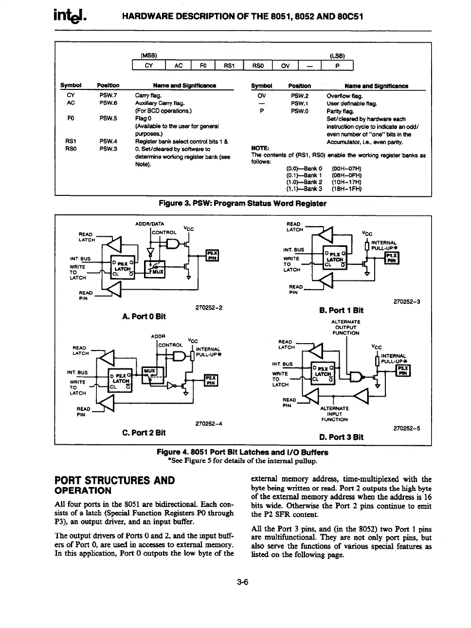
Figure 3. PSW:Program Status Word Register
AODR/OATA
READ
LATCH
INT.BuS
WRITE
TO
LATCH
REAO
PIN
2702S2-2
A. PorfOBit
P.oon
Vcc
READ
CONTROL
LATCH
INT.BuS
WRITE
TO
d
LATCH
REAO
PIN
270252-4
C. Port 2 Bit
270252-3
B. Port 1 Bit
ALTERNATE
OUTPUT
FUNCTION
-.
FUNCTION
270252-5
D. Port 3 Bit
Figure 4.8051 Port Bit Latches and 1/0 Buffers
*See
Figure5for detailsofthe internalpultup.
PORTSTRUCTURESAND
OPERATION
AUfour ports in the 8051are bidirectional.Each con-
sists of a latch (SpecialFunction
Regietera PO through
P3), en outputdriver,and an input buflkr.
TheoutputdriversofPortsOand2, andthe inputbutF-
era of Port O,are usedin ameaaes
to externalmemory.
In this application,Port Ooutputs the lowbyte of the
external memory addres3,time-multiplexedwith the
bytebeingwrittenor read. Port 2 outputsthe highbyte
of the externalmemoryaddress whenthe addressis 16
bits wide. Otherwisethe Port 2 pine continue
to emit
the
P2 SFR content.
All the Port 3 pina,and (in the 8052)two Port 1pins
are multifunctional.They are not onfy port pins, but
afao serve the functionsof various special featureaas
listedon the followingpage.
3-6