i~e
HARDWAREDESCRIPTION OF THE 8051,8052 AND 80C51
he
w
70 m?lsmu
F5
nsaNo curs
m
%s
---- —---
xrMl----- xrAL2------
I
w v
1
c1
Q
=
270252-27
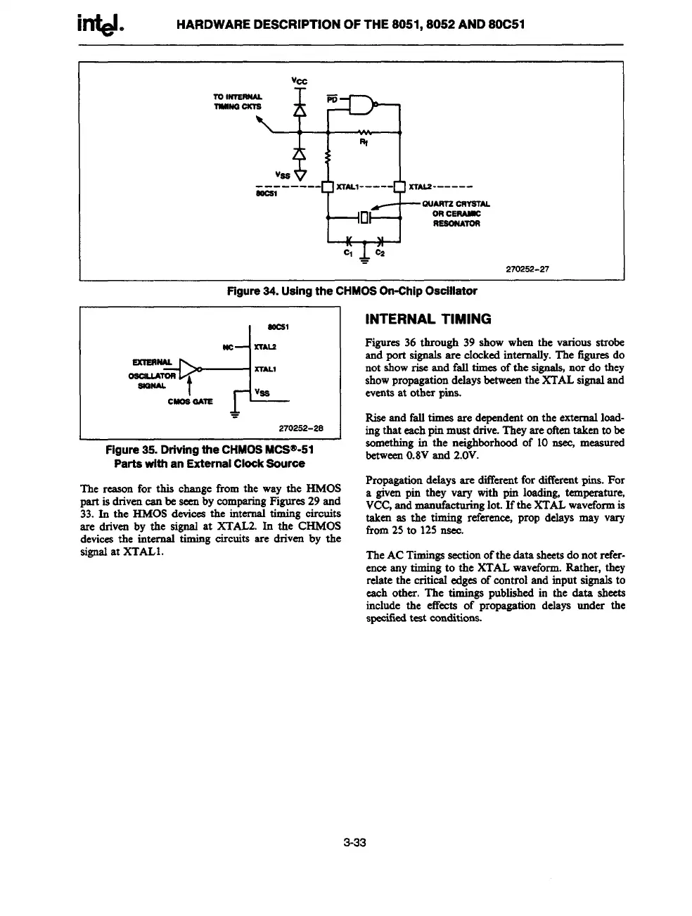
Figure 34. Usingthe CHMOS On-ChipOscillator
I
Soeal
MC+ X-rAu
*
270252-28
Figura 35. Driving the CHMOS MCS@’-5l
Parts with an External Clock Source
The reason
for this change from the way the HMOS
part is drivencan be seenbycomparingFigures29and
33. In the HMOS devicesthe internal timing oircuits
are driven by the signal at XTAL2. In the CHMOS
devicesthe internal timing circuits are driven by the
signalat XTAL1.
INTERNALTIMING
Figures 36 through 39 show when the variousstrobe
and port signalsare clockedinternally.The figuresdo
not showrise and fall timesof the signals,nor do they
showpropagationdelaysbetweentheXTALsignaland
eventsat other pins.
Riseand fall times are dependenton the externalload-
ingthat eachpin must drive.Theyare oftentakentobe
somethingin the neighborhoodof 10~ measured
bemveen0.8Vand 2.OV.
Propagationdelaysare differentfor differentpins. For
a givenpin they vary with pin loading temperature,
VCC,andmanufacturinglot. If the XTALwaveformis
taken as the timing referenee,prop delays may vary
from25to 125nsec.
TheACTimingssectionofthe data sheetsdonot refer-
enceanytimingto the XTALwaveform.Rather, they
relate the criticsdedgesof control and input signalsto
eaohother. The timings publishedin the data sheets
include the effects of propagation delays under the
specitledtest conditions.
3-33