intel.
MCS@-51 ARCHITECTURAL OVERVIEW
Data Memory occupies a separate addrexs space from
%OgrCt122 hkznory. Up to 64K bytes of exterttd RAM
can be addreased in the externrd Data Memo~.
The CPU generatea read and write signals RD and
~, as needed during external Data Memory accesses.
External Program Memory and external Data Memory
~~ combined if-desired by applying the ~ ~d
PSEN signals to the inputs of an AND gate and using
the output of the gate as the read strobe to the external
Program/Data memory.
ProgramMemory
Figure 3 shows a map of the lower part of the Program
Memory. After reset, the CPU begins execution from
location OWOH.
AS shown in F@ure 3, each interrupt is
assigned a tixed
location in Program Memory. The interrupt causes the
CPU to jump to that location, where it commences exe-
cution of the serviee routine. External Interrupt O, for
example, is assigned to location 0003H. If External In-
terrupt O is going to & used, its service routine must
begin at location 0003H. If the interrupt is not going to
be used, its service location is available as general pur-
pose Program Memory.
i
..-.
INTSRRUPT
LOCATIONS
R2S~
&
(O033H)
002EH
002SH
00IBH
II
Ssvrm
0013H
000SH
0003H
0000H
270251-3
Figure 3. MCW’-51 Program Memory
The interrupt aeMce locations are spaced at 8-byte in-
tervak 0U03H for External Interrupt O, 000BH for
Tmer O, 0013H for External Interrupt 1, 00IBH for
Timer 1, etc. If an interrupt service routine is short
enough (as is often the case in control applications), it
can reside entirely within
that 8-byte interval. Longer
service routinea can use a jump instruction to skip over
subsequent interrupt locations, if other interrupts are in
use.
The lowest 4K (or SK or 16K) bytes of Program Mem-
ory can be either in the on-chip ROM or in an external
ROM. This selection is made by strapping the ~ (Ex-
ternal Access) pin to either VCC or Vss.
In the 4K byte ROM devices, if the= pin is strapped
to VcC, then program fetches to addresses 0000H
through OFFFH are directed to the internal ROM. Pro-
gram fetches to addresses 1000H through FFFFH are
directed to external ROM.
In the SK byte ROM devices, = = Vcc selects ad-
dresses (XtOOHthrough lFFFH to be internal, and ad-
dresses 2000H through F’FFFH to be external.
In the 16K byte ROM devices, = = VCC selects ad-
dresses 0000H through 3FFFH to be internal, and ad-
dresses 4000H through FFFFH to be external.
If the ~ pin is strapped to Vss, then all program
fetches are directed to external ROM. The ROMleas
parts must have this pin externally strapped to VSS to
enable them to execute properly.
The read strobe to externally: PSEN, is used for all
external oro.cram fetches. PSEN LSnot activated for in-
‘s
l==
m%
1
Po
m
=
ALE
LArcn
EPROM
INSTR.
1
AOOR
a’s ‘z~
270251-4
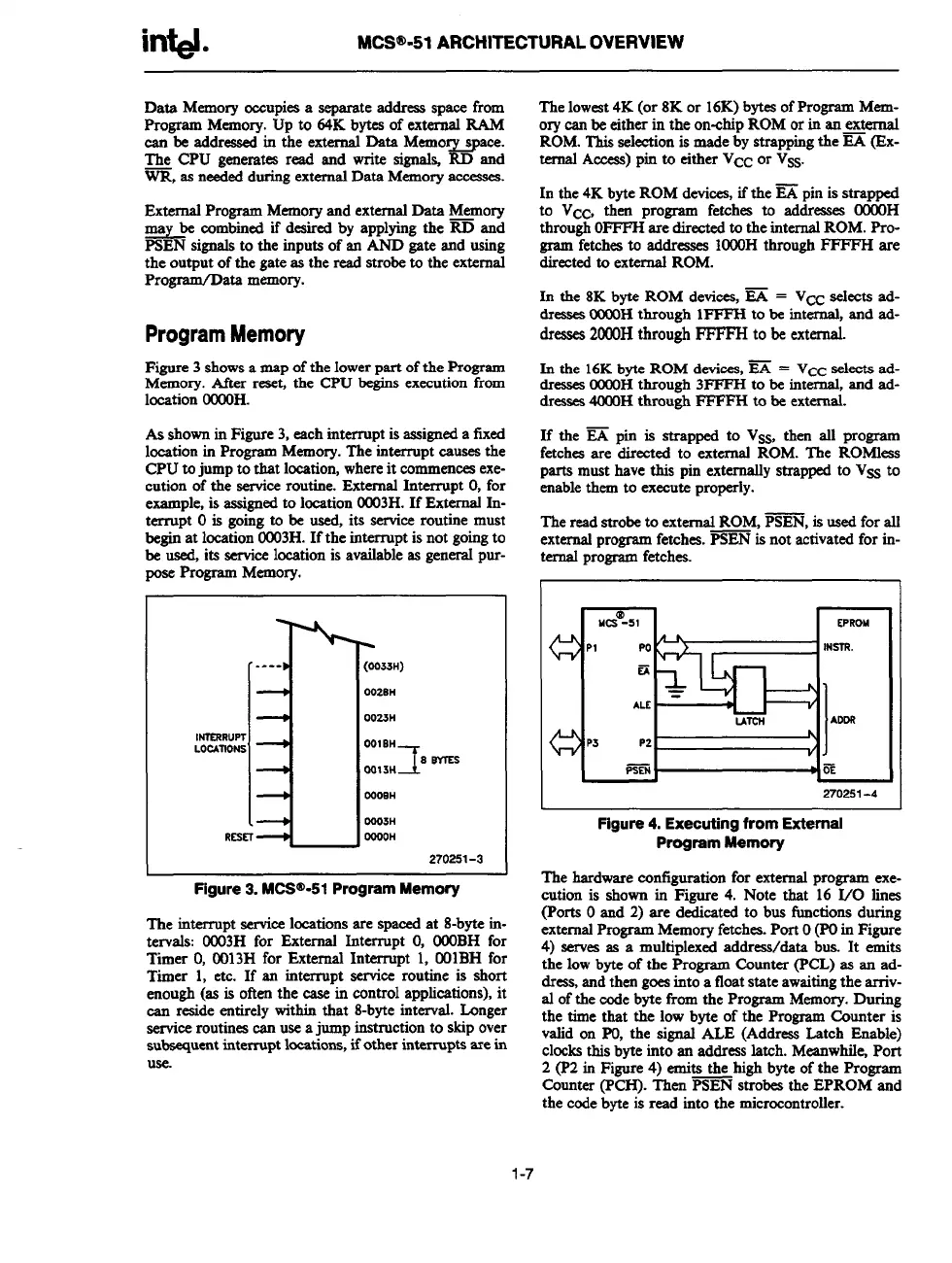
Figure 4. Executing from External
Program Memory
The hardware configuration for external program exe-
cution is shown in Figure 4. Note that 16 I/O lines
(Ports O and 2) are dedicated to bus fictions during
external Program Memory f~hes. Port O(POin Figure
4) servex as a multiplexed address/data bus. It emits
the low byte of the Program Counter (PCL) as an ad-
dress, snd then goes into a float state awaiting the arriv-
al of the code byte from the Program Memory. During
the time that the low byte of the Program Counter is
valid on PO, the signal ALE (Address Latch Enable)
clocks this byte into an address latch. Meanwhile, Port
2 (P2 in Figure 4) emits the high byte of the Program
Countex (WI-I). Then ~ strobex the EPROM and
the code byte is read into the microcontroller.
1-7