MCS@-51 ARCHITECTURAL OVERVIEW
Program Memory addresses are always 16 bits wide,
even though the aotual amount of Program Memory
used ntSy be kSS than 64K bytes. External prOq
exeoutiorssacrifices two of the 8-bit ports, POand P2, to
the fisnction of addressing the Program Memory.
Data Memory
Theright
half of Figure 2 shows the internal and exter-
nal Dats Memory spaces available to the MCS-51 user.
F@ure 5 shows a hardware configuration for accessing
up to 2K bytes of external RAM. The CPU in this ease
is executing from internal ROM. Port O serves as a
multiplexed address/data bus to the RAM, and 3 lines
of Port 2 are bein~d to page the RAM. The CPU
generates = and WR signals as needed during exter-
ial WM
ameases. -
1’
I
I
270251-5
Figure 5. Accessing External Data Memory.
If the Program Memory is Internal, the Other
Bits of P2 are Available as 1/0.
There ean be up to 64K bytea of external Data Memo-
ry. External Data Memory addresses can be either 1 or
2 bytes wide. One-byte addresses are often used in cxm-
junction with one or more other 1/0 lines to page the
R4M, as shown in Figure 5. Two-byte addresws ears
atso be used, irz which case the high address byte is
emitted
at Port 2.
~:.. .-... -
EP
FFH
, AC=IELE ACCESSIBLE
UPP~ , SV INDIREC7 BV OIRECT
: AtORESSING AODRSSSING
ONLY
SDH9 80H
‘m ACCESSIBLE
LOWER
SY 01REC7
SPWAL
128
ANO INC+REC7
1
W
NC710N &oAmm~o
o AGGRESSING
‘E~m CONTROLems
TIMER
RE—
STACKiolN7ER
ACCUMULATOR
(’nC.)
270251-6
Figure 6. Internal Data Memory
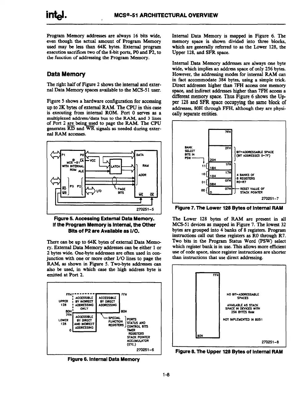
Internal Data Memory is mapped in Figure 6. The
memory space is shown divided into three bloeka,
which are generally referred to as the Lower 128, the
Upper 128, and SFR space.
Internal Data Memory addresses are always one byte
Wid%which implies an address space of only 256 bytes.
However, the addressing modes for intemssl RAM ean
in fact seeommodate 384 bytes, using a simple trick.
Direct addresses higher than 7FH awes one memory
space, and indirect addresses higher than 7FH access a
different memory space. Thus Figure 6 shows the Up-
per 128and SFR
spaceoccupyingthe ssmeblockof
addrq
80H throu~ FFH, slthoud they are physi-
cally separateentities;
n
7FH
BANK
Ill
2FH
SELECT
BRS IN
1
SN-ACORESSASLSSPACE
(S~ A~ESSES O-7F)
‘1 20H
“{ lSH
1FH
‘0{ 10H
17H
4 SANKSOF
8 REGIS7SRS
0’{ OBH
OFH
RO-R7
eo{o
07H RESETVALUEOF
S7ACKPOIN7ER
270251-7
Figure 7. The Lower 128 Bytes of internal RAM
The
Imwer 128 bytes of W are present in all
MCS-51 devices as mapped in F@ure 7. The lowest 32
bytes are grouped into 4 banks of 8 registers. Program
instructions call out these registers as RO through R7.
Two bits in the Program Status Word (PSW) seleet
which register bank is in use. This allows more effieient
use of code space, since register instructions are shorter
than instructions that use direet addreasiig.
I
FFH
80H
NO SIT-AOORSSSABLE
SPACES
AVAIUBLE AS S7ACK
SPACEIN DEVICESWMI
256 BWES RAM
NOTIMPLE14EN7EDIN 8051
270251-8
Figure 6. The Upper 128 Bytes of Internal RAM
I-6