8XC51FXHARDWAREDESCRIPTION
B. Port 1 or Porl 3 Bit
ALTERNATE
OUTPUT
FUNCTION
h’
CONTROL
Vcc
i
i
El
Y
+
wRITE
-+
Iu
wl—
TO
LATCH
~—
A. PortOBit
ADDRIOATA
READ
*
LATCH
READ
LATCH
INT.BUS
‘.%: -C T
NRITE
INT.BUS
ro
CL
.ATCH
REAO
PIN
ALTERNATE
INPUT
FUNCTION
270W3-4
270653-2
C.Port 2 Bit
ADDR
----
kONTRoL ‘?c ---
“tALl
LATCH
INT,MN
LATCH
WRITE
1
- CL
TO
E
LATCH
READ~
PIN
●SeeFiwre4fordetails of the internal pullup
270653-3
—.
——.—.. — . .. . . .. .- - ..
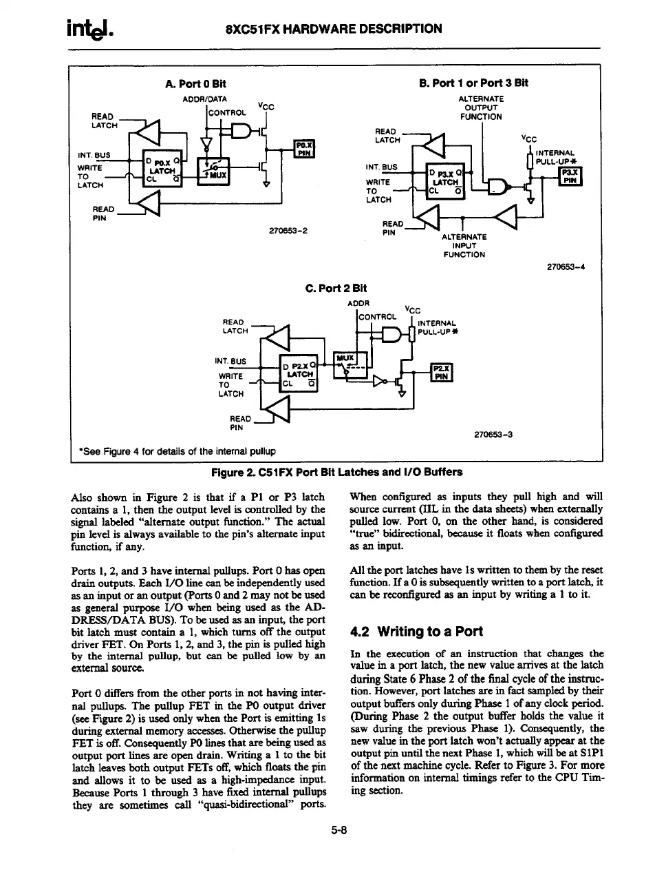
Figure 2. C51FX Port Bit Latcnes ana vw 6urrera
Also shown in Figure 2 is that if a PI or P3 latch
contains a 1. then the outrmtlevel is controlled by the
signal label~
“alternate output function.” The a-~usl
pin level is always availableto the pin’s akernate input
functiom if any.
Ports 1, 2, and 3 have internalpullups. Port Ohas open
drainoutputs. Each 1/0 line canbe independentlyused
as an input or an output (PortsOand 2 may not be used
= general P- 1/0 when being used as the ~-
DRESWDATA BUS). To be usedas an input, the port
bit latch must contsin a 1, which turns off the output
driverFET. On Ports 1,2, and 3, the pin is pulled high
by the internal pullup, but can be putled low by an
external
source.
Port Odiffers from the other portsin not having inter-
nal pullups. The ptdlup PET in the POoutput driver
(see Figure 2) is used only when the Port is emitting 1s
duringexternal memory accesses.otherwise the pullup
PET is off. Cawqucrttly POlinesthat arebeing used as
output port lines are open drain. Writing a 1 to the bit
latch leaves both output FETs off, which floats the pin
and allows it to be used as a high-impedance input.
Because Ports 1 through 3 have fixed internal pullups
they are sometimes call “quasi-bidirectional” ports.
When configured as inputs they pull high and will
source curren
t (IIL in the data sheets) when externally
pulled low. Port O, on the other hand, is considered
“true” bidirectional,because it floats when configured
as an input.
Ml the port latcheshave 1swritten to themby the reset
function. If a Ois subsequentlywrittentoa portlatch, it
can be recotrtljuredas an input by writinga 1 to it.
4.2 Writing to a Port
In the execution of an instruction that changes the
value in a port latch, the new value arrivesat the latch
during State 6
Phase2of thefinalcycleoftheinstrtrc-
tion. However,port latches arein fact sampledby their
output btiers only during Phase 1 of any clock period.
(During Phase 2 the output butlsr holds the value it
saw during the previous Phase 1). Consequently, the
new valuein the port latch won’t actuallyappearat the
output pin until the next Phase 1, which will be at SIP1
of the next machine cycle. Refer to Figure3. For more
informationon internal timings referto the CPU Tim-
ing section.
5-8