i@L
8XC51FX HARDWARE DESCRIPTION
4.3 Port Loading and Interfacing
The output bfiers of Ports 1, 2, and 3 can each sink
1.6 MA at 0.45 V. These port pil13can be dliVeIlby
open-collector and open-drain outputs although o-to-l
transitions will not be fast since there is little current
pulling the pin up. An input Oturns off pullup pFET3,
leaving only the very weak pullup pFET2 to drive the
transition.
In external bus mode, Port O output buffers can each
sink 3.2 MA at 0.45 V. However, as port pins they
requireexternalpullups to be able to drive any inputs.
Sec the latest revision of the data sheet for design-in
information.
4.4 Read-Modify-Write Feature
Some instructions that read a port read the latch and
othersreadthe pin. Which ones do which? The instruc-
tions that readthe latch ratherthan the pin arethe ones
that reada VAIU%possibly changeit, and then rewriteit
to the latch. These are called “read-modify-write”in-
structions. Listed below are the read-modify-writein-
structions. When the destination operandis a port, or a
port bit, these instructions read the latch rather than
the pin:
ANL (logical AND, e.g., ANL Pl, A)
ORL
(logical OR, e.g., ORL P2, A)
XRL (logical EX-OR, e.g., XRL P3, A)
JBc (jump if bit = 1 and clear bit, e.g.,
JBC P1.1, LABEL)
CPL (complement bit, e.g., CPL P3.0)
INC (increment, e.g., INC P2)
DEC
(decrernen~ e.g., DEC P2)
DJNZ
(decrementand jump if not zero, e.g.,
DJNZ P3, LABEL)
MOV, PX.Y, C (move carrybit to bit Y of Port X)
CLR PX.Y (clear bit Y of Port X)
SETB PX.Y
(setbit Y of Port X)
It is not obvious that the last three instructions in this
list are read-modify-write instructions, but they are.
They readthe portbyte, all 8 bits, modify the addressed
bit, then write the new byte back to the latch.
The reason that read-modify-writeinstructions are di-
rected to the latch rather than
the pin is to avoid a
possible
misinterpretation of the voltage level at the
pin. For example, a port bit might be used to drive the
base of a t
ransiator.When a 1 is written to the bit, the
transistoris turned on. If the CPU then reads the same
port bit at the pin ratherthan the latch, it will readthe
base voltage of the transistorand interpret it as a O.
Reading the latch rather than the pin will return the
correctvalue of 1.
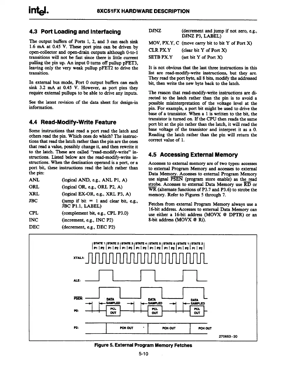
4.5 Accessing External Memory
Accesses to externalmemory areof two types:accesses
to externrdProgram Memory and acccases to external
Data Merno~Accesses to external Program Memory
use signal PSEN (program store enable) as the read
strobe. Accesam
to external Data Memory use ~ or
~ (alternatefunctions of P3.7 and P3.6) to strobethe
memory. Refer to Figures 5 through 7.
Fetches from external ProgramMemory always use a
lfibit address. Accesses to externalData Memory can
use either a 16-bit address (MOVX @ DPTR) or an
8-bit address (MOVX @Ri);
=A~ 1 =A’= 2 STATE3 STATS4 STATES ~ATS 6 STATS1 STATS2
IPtlnlP!lmlmlnl Ptlmlmlml Pl,nlPllmlFllnl
ATAL1:
ALE, ~
~:
OATA OATA
--l
+~ +SAMPLSO
PO:
z
,
P2:
PCHOU7 .
Pcnolrr Pmour
270S53-30
Figure 5. External Program Memory Fetches
5-1o