i@.
8XC51FXHARDWAREDESCRIPTION
4.0 PORT STRUCTURES AND
OPERATION
All
four ports in the C51FX are bidirectional. Wch
consists of a latch (Special Function Registers PO
through P3), an output driver,and an input buffer.
The output driversof PortsOand 2, and the input buK-
ers of Port O,are used in accessesto externalmemory.
In this application, Port Ooutputs the low byte of the
external memory address, time-multiplexed with the
byte being written or read.Port 2 outputs the high byte
of the external memory address when the address is
16bits wide. Otherwisethe Port2 pins continue to emit
the P2 SFR content.
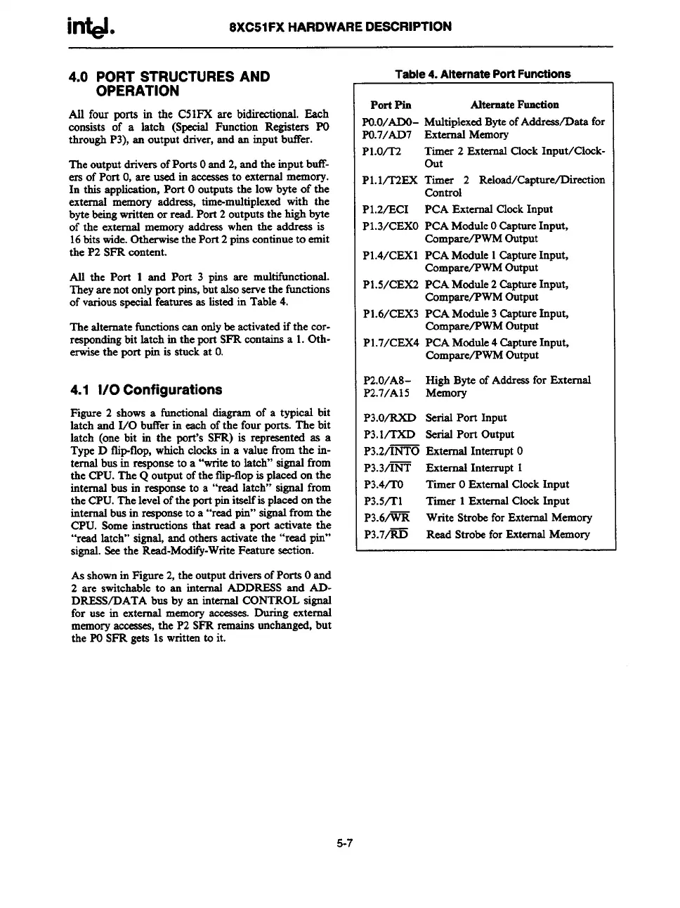
All the Port 1 and Port 3 pins are multifimctional.
They arenot only port pins, but also servethe functions
of variousspecial featureaas listed in Table 4.
The alternatetimctions can onlybe activatedif the cor-
respondingbit latch in the port SFR contains a 1. Oth-
erwise the port pin is stuck at O.
4.1 1/0 Configurations
Figure 2 shows a functional diagram of a typical bit
latch and I/O butTerin each of the four ports. The bit
latch (one bit in the port’s SFR) is represented as a
Type D flipflop, which clocks in a value from the itt-
ternalbus in response to a “writeto latch” signal from
the CPU. The Q output of the flip-flop is placed on the
internal bus in response to a “read latch” signal from
the CPU. The level of the portpin itself is placedon the
internalbus in response to a “readpin” signal from the
CPU. Some instructions that read a pert activate the
“read latch” signal, and others activate the “read pin”
signal. See the Read-Modify-WriteFeature section.
Table 4. Alternate Port Functions
Port Pin
AlternatePunction
PO.O/ADO-Multiplexed Byte of Address/Data for
PO.7/AD7 External Memory
P1.OA--2
Timer 2 External Clock Input/Clock-
Out
P1.1/TX3X Timer 2 Reload/Capture/Direction
Control
P1.2/ECI PCA External Clock Input
P1.3/CEXO PCA Module OCaptureInput,
Compare/PWM Output
P1.4/CEXl PCA Module 1 CaptureInput,
Compare/TWM Output
P1.5/CEX2 PCA Module 2 CaptureInput,
COmpare/PWMOutput
P1.6/CEX3 PCAModule 3 CaptureInpuL
Compare/PWM Output
P1.7/CEX4 PCA Module 4
Capture Input,
Compare/PWM Output
P2.O/A8- High Byte of Address for External
P2.7/A15
hiemory
P3.O/RXD Serial Port Input
P3,1iTXD Serird
port Output
P3.2/INTO External InterruptO
P3.3/INT ExternaI Interrupt 1
P3.4/To
Timer OExternal Clock Input
P3.5fll Timer 1 ExternalClock Input
P3.6~ Write Strobe for ExternalMemory
P3.7m
Read Strobe for ExternalMemory
As shown in Figure 2, the outputdriversof Ports Oand
2 are switchable to an internal ADDRESS and AD-
DRESYDATA bus by an internal CONTROL signal
for use in external memory
aecmaes. During external
memory accesses,
the P2 SFR remains unchanged, but
the POSFR gets 1s written to it.
5-7