it@le
8XC52/54/58 HARDWARE DESCRIPTION
Finally, for a master to communicate with both slaves
at once the addressmust have bit O = 1and bit 1 = O.
Notice, however, that bit 2 is a don’t-care for both
slaves. This allows two difTerentaddresses to select
both slaves (1111 0001 or 11110101). If a third slave
was added that requiredits bit 2 = O,then the latter
addreascould be used to communicate with Slave 1and
2 but not Slave 3.
The master can also communicate with all slaves at
once with the BroadcastAddress. It is formed from the
logical OR of the SADDR and SADEN registerswith
zeroes defined as don’t-cares. The don’t-caresalso al-
low flexibility in defiig the BroadcastAddress, but in
most applications a BroadcastAddress will be OFFH.
SADDR and SADEN arelocated at addressOA9Hand
OB9H, respectively. On reset, the SADDR and
SADEN registers are inidalized to OOHwhich defines
the Oiven and BroadcastAddresses as XXXX XXXX
(all don’t-cam). This assuresthe 8XC5X serialport to
be backwards compatible with other MCS@-51prod-
ucts which do not implement automatic addressrecog-
nition.
INTERRUPTS
The
8XC5X hasa total of 6 interrupt vectors:two ex-
——
ternal interrupts (INTO and INT1), three timer inter-
rupts (Timers O, 1 and 2) and the serial port interrupt.
These interruptsare all shown in Figure 6.
Tinter2 Interruptis generatedby the logical OR of bits
TF2 and EXF2 in register T2CON. Neither of theae
flags is clearedby hardwarewhen the scMce routine is
vectored to. In fact, the service routine may have to
determinewhether it was TF2 or EXF2 that generated
the intemupt and that bit will have to be cleared in
software.
The TimerOandTimer 1flags,TFOand TF1, areset at
S5P2 of the cycle in which the tinters overtlow. The
valuesarethen polled by the circuitryin the next cycle.
However, the Timer 2 tlag, TF2 is set at S2P2 and is
polled in the same cycle in which the timer overflows.
Interrupt Priority Structure
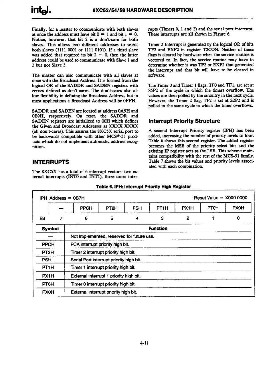
A seumd Interrupt Priority register (ET-I) has been
added, increasingthe number of prioritylevels to four.
Table 6 shows this second register.The added register
becomes the MSB of the priority select bits and the
existing 1Pregisteracts as the LSB. This scheme main-
tains compatibility with the reatof the MCS-51 family.
Table 7 shows the bit values and prioritylevels associ-
ated with each combination. “
.- -
IPH Address= OB7H ResetValue= XOOO0000
—
PPCH PT2H
PSH
PTIH
PXIH PTOH
PXOH
Bit
7 6
5
4 3 2 1
0
Symbol
Function
—
NotImplemented,reservedforfutureuse.
PPCH PCAinterruptpriorityhighbit.
PT2H
Timer
2 interruptpriority high bit.
PSH serial Port interrupt priority high bit.
PTIH
Timer1interruptpriorityhighbit.
PXIH Externalinterrupt1priorityhighbit.
PTOH
TimerOinterruptpriorityhighbit.
PXOH
Externalinterruptpriorityhighbit.
4-11