irrtel.
MCS@-51 ARCHITECTURAL OVERVIEW
Logical Instructions
Table 3 shows the list ofMCS-51 logical instructions.
The instructions that perform Boolean operations
(AND, OIL Exclusive OIL NOT) on bytes perform the
operation on a bit-by-bit bssis. That is, if the Aecumu-
Iator contains 001101OIB and <byte> contains
O1OIOOIIB,then
ANL
A, <byte>
will leave the Accumulator holding OOO1OOOIB.
The addrcasing modes that can be used to access the
<byte> operand are
listedinTable 3. Thus, the ANL
A, <byte> instruction may take any of the forms
ANL A,7FH (direct addressing)
ANL A,@Rl
(indirect addressing)
ANL
A,R6 (register addressing)
ANL
A, # 53H (immediate constant)
AU of the logical instructions that are Accumulator-
specflc execute in lps (using a 12 MHz clock). The
othem take 2 ps.
Note that Boolean operations can be performed on any
byte in the lower 128 internal Data Memory space or
the SFR space using direct addressing, without having
to use the Accumulator. The XRL <byte >, #data in-
struction, for example offets a quick and easy way to
invert port bits, as in
XRL Pl,#oFFH
If the operation is in response to an interrupt, not using
the Accumulator saves the time and effort to stack it in
the service routine.
The Rotate instructions (3U & RLC A, etc.) shift the
Aeeurtmlator 1 bit to the MI or right. For a left rota-
tion, the MSB rolls into the LSB position. For a right
rotation, the LSB rolls into the MSB position.
The SWAP A instruction interchanges the high and
low nibbles within the Accumulator. This is a useful
operation in BCD manipulations. For exampie+ if the
Accumulator contains a binary number which is known
to be leas thsn IQ it can be qnickly converted to BCD
by the following code:
MOV B,# 10
DIV AB
SWAP A
ADD A,B
Dividing the number by 10 leaves the tens digit in the
low nibble of the Accumulator, and the ones digit in the
B register. The SWAP and ADD instructions move the
tens digit to the high nibble of the Accumulator, and
the onea digit to the low nibble.
Data Transfers
INTERNAL RAM
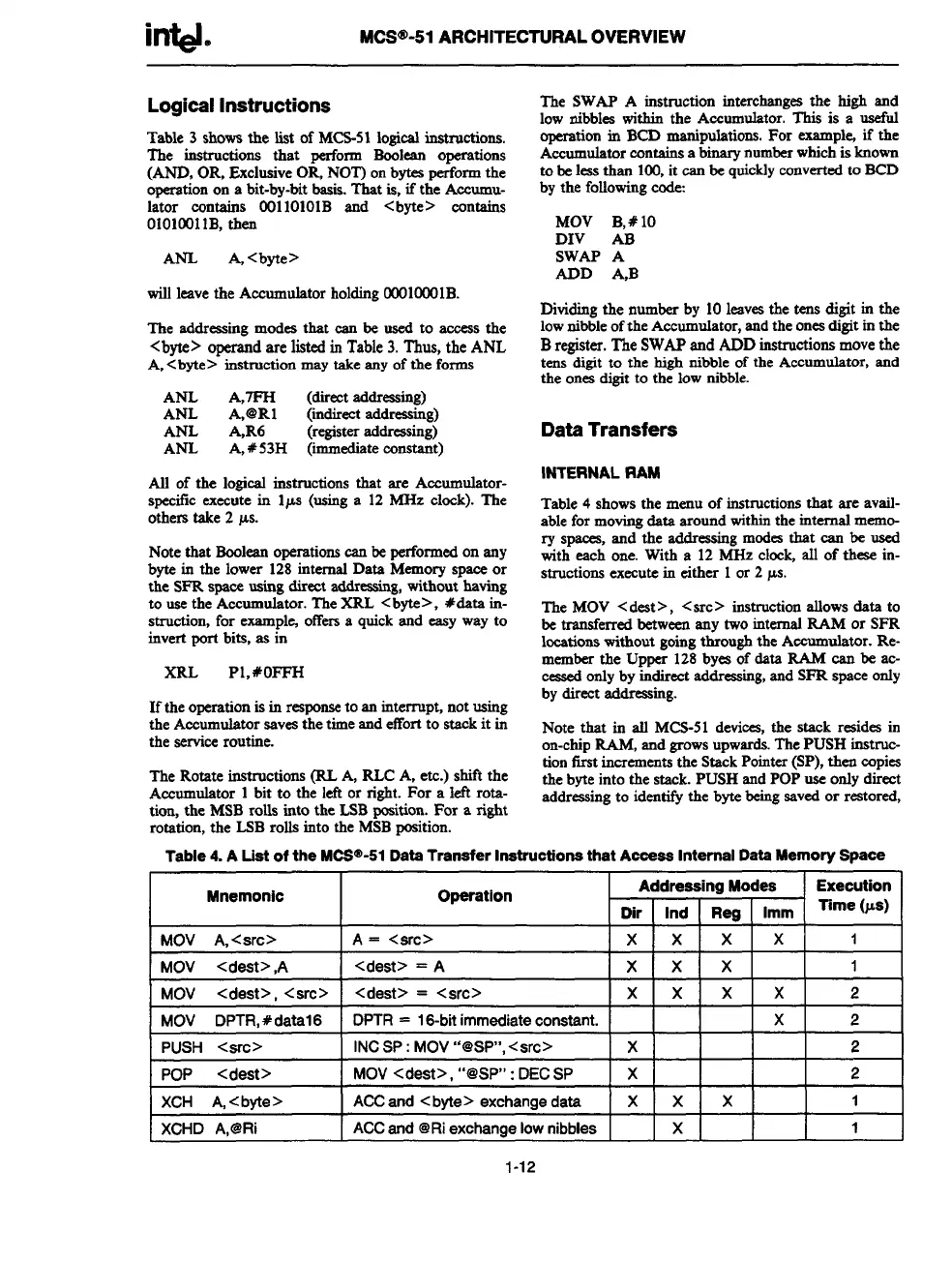
Table 4 shows the menu of instructions that are avail-
able for moving data around within the internal memo-
ry spaces, and the addressing modes that can be used
with each one. Wkh a 12 MHz clock, all of these in-
structions execute in either 1 or 2 ps.
The MOV < dest>, < src > instruction allows dats to
be transferred between any two internal RAM or SFR
lwations without going through the Accumulator. Re-
member the Upper 128 byes of data RAM can be ac-
wased only by indirect addressing, and SFR space only
by direct addressing.
Note that in all MCS-51 devices, the stack resides in
on-chip RAM, and grows upwards. The PUSH instruc-
tion first increments the Stack Pointer (SP), then copies
the byte into the stack. PUSH and POP use only dkcct
addressing to identify the byte being
saved or restored,
Table 4. A List of the MCS@-51 Data Tranafer Instructions that Access Internal Data Memory Space
Mnemonic Operation
Addressing Modes
Execution
Dir
Ind Reg
Imm
Time (ps)
MOV A, <src>
A = <src>
x x x x
1
MOV <cleat> ,A
<dest> = A
x x x
1
MOV <dest>, <src>
<dest> = <src>
x x x x
2
MOV DPTR,#data16
DPTR = 16-bit immediate constant.
x
2
PUSH <WC>
INCSP: MOV “@’SP’, <src>
x
2
POP
<dest>
MOV <dest>, “@SP”: DECSP x
2
XCH A,<byte>
ACCand <byte> exchange data
x x x
1
XCHD A,@Ri
ACCand @Riexchange low nibbles
x
1
1-12