i~.
M~@.51 ARCHITECTURAL OVERVIEW
PROORAMMrhtosv
(REM ONLY)
* ----------- --------------
8
1
1
1
1
1
1
1
I
1
I
o
8
0
0
0
8
0
0
9
I
I
I
,
1
I
:
#
o
0
1
0
@
*
I
:
● -
FFFFw
$
s
I
1
1
T -
1
1
1
1
1
1
1
1
EXTERNAL
1
1
1
1
1
I
1
1
1
I
,
B
I
I
G=o m.1
:
2STERNAL
IN7ERNAL :
0
9
*
I
0000
I
I
--- -------- -------- -.!
OATAMEMORY
(RW/WRlT2)
------------------------ . . . . .
t
8
8
8
I
1
I
I
I
8
0
I
I
I
*
I
0
I
EXIERNALm
:
I
#
o
I
#
I
8
I
9
I
8
-
I
8
0
I
1
0
9
t
:
1
#
I
I
I
,
1
IN7ERNM
I
: FfH: ------
,1+
J:
1
0:
I
9,
e,
1
9
0
1
9
8
0
1
1
I 00
0000
1
1
●-------- --------- ..- -. -.-:
1% tiR
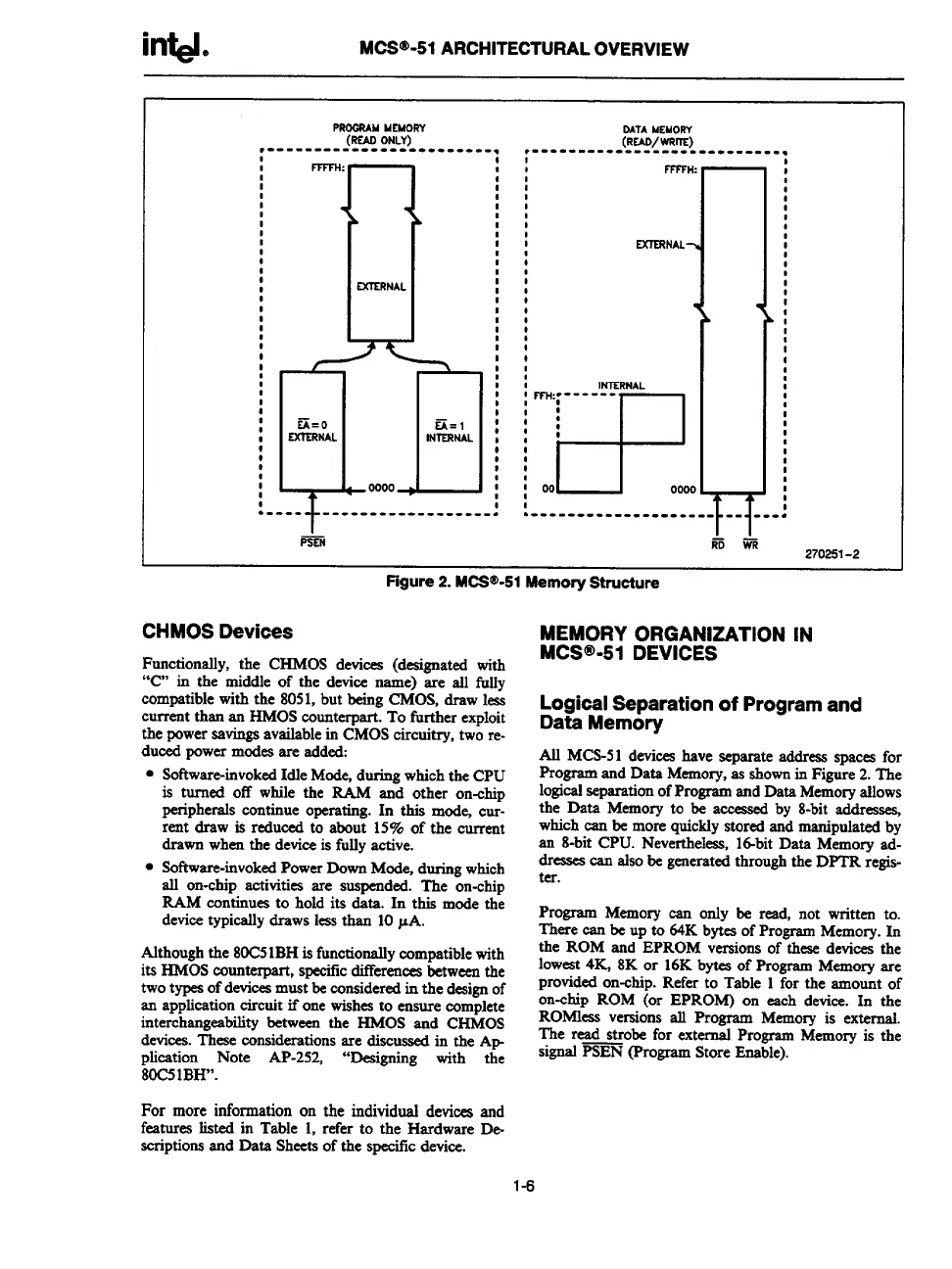
Figure 2. MCW’-51 Memory Structure
CHMOS Devices
Functionally, the CHMOS devices (designated with
“C” in the middle of the device name) me all
fiuy
compatible with the 8051, but being CMOS, draw less
current than an HMOS counterpart. To further exploit
the power savings available in CMOS circuitry, two re-
duced power modes are added
● Software-invoked Idle Mode, during which the CPU
is turned off while the RAM and other on-chip
peripherals continue operating. In this mode, cur-
rent draw is reduced to
about 15% of the current
drawn when the device is fully active.
● Software-invoked Power Down Mode, during which
all on-chip activities are suspended. The on-chip
RAM continues to hold its data. In this mode the
device typically draws less than 10 pA.
Although the 80C51BH is functionally compatible with
its HMOS counterpart, s~lc differeneea between the
two types of devices must be considered in the design of
an application circuit if one
wiahea to ensure complete
interchangeability between the HMOS and CHMOS
devices. These considerations are discussed in the Ap
plieation
Note AP-252, “Designing with the
80C5lBH.
For more information on the individual devices and
features listed in Table 1, refer to the Hardware De
scriptions and Data Sheets of the specific device.
270251-2
MEMORY ORGANIZATION IN
MCS@-51 DEVICES
Logical Separation of Program and
Data Memory
AU MCS-51 devices have separate address spacea for
Program and Data Memory, as shown in Figure 2. The
logical separation of Program and Data Memory allows
the Data Memory to be acceased by 8-bit addressea,
which can be more quickly stored and manipulated by
an 8-bit CPU. Nevertheless, ld-bh Data Memory ad-
dresses can also be generated through the DPTR regis-
ter.
Program Memory can only be read, not written to.
There can be up to 64K bytes of Program Memory. In
the ROM and EPROM versions of these devices the
loweat 4K, 8K or 16K bytes of Program Memory are
provided on-chip. Refer to Table 1 for the amount of
on-chip ROM (or EPROM) on each device. In the
ROMleas versions all Program Memory is external.
The read strobe for external Program Memory is the
signal PSEN @rogram Store Enable).
1-6