intd.
8XC51FXHARDWAREDESCRIPTION
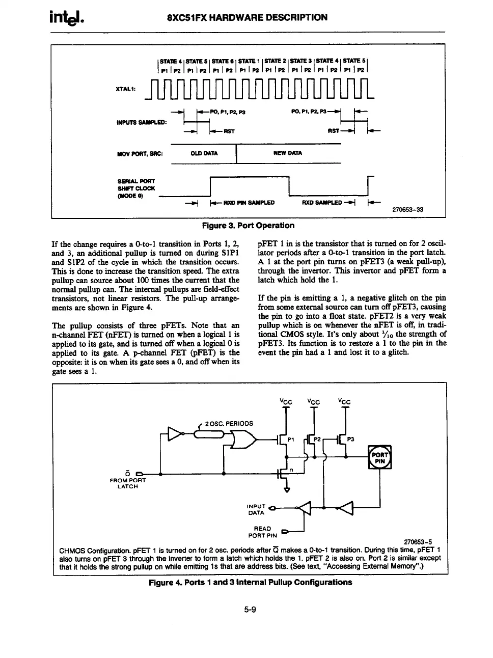
SIAIS 4 STATS5 STATS6 STATS1 6TATS2 STATS3 STATS4 STATS5
lmlnlmlmlmlmImlmlPllmlmlmlHlmlmd
XTALI:
-–’mp:” “’”’’””MI
NOVPONT, SRC:
OLOOATA
I
NSWOATA
270S53-33
I
Figure 3. Port Operation
If the change requireaa O-to-1transition in Porta 1, 2,
and 3, an additional pullup is turned on duxing SIP1
and S1P2 of the cycle in which the transition occurs.
This is done to increasethe transition speed. The extra
pullup can source about 100 times the currentthat the
normal pullup can. The internal pollups are field-effect
transistors, not linear resistors. ‘l%epull-up arrange-
ments are shown in Figure 4.
pFET 1in is the transistorthat is turnedon for 2 oscil-
lator periodsaftera o-t~l transition in the port latch.
A 1 at the port pin turns on pFET3 (a weak pull-up),
through the invertor. This invertor and pFET form a
latch which hold the 1.
If the pin is emitting a 1, a negative glitch on the pin
from some externalsource can turn off pFET3, causing
the pin to go into a float state. EFET2 k a very weak
The pullup consists of three pFETs. Note that an pullup whi;h is on whenever th; nFET is off, ~ tradi-
n-channel FET (r@ET)is turned on when a logical 1is
tional CMOS style. It’s onIy about Y,Othe strength of
applied to its gate, and is turned off when a logical Ois
pFET3. Its futtction is to restore a 1 to the pin in the
applied to its gate. A p-channel FET (pFET) is the
event the pio had a 1 and lost it to a glitch.
opposite:it is on when its gate sees a O,and offwhen its
gate sees a 1.
Vcc
‘JCc
Vcc
TTT
PI
()
6 D
n
FROM PORT
LATCH
I
INPUT
~
J
DATA
“A” DJ
PORT PIN
270S53-5
2HMOS Configuration. pFET1iaturnedonfor2OSC.periodaafter~ makeaaO-to-1transition.Duringthistime,pFEr1
alsoturnsonPFET3throughtheinvertertoforma latchwhichholdathe1.PFET2 isalsoon.Port2issimilarexcept
thatit
holdathe strongDUIIUIIon whileemitting1s that are addreaabits.(See text, “AcceaaingExternalMemory”.)
—
. - . .—.. — .. ..
Figure 4. Ports 1 artct3 Internal Pullupconfigurations
5-9