intele
8XC51FXHARDWAREDESCRIPTION
14.0 ON-CHIP OSCILLATOR
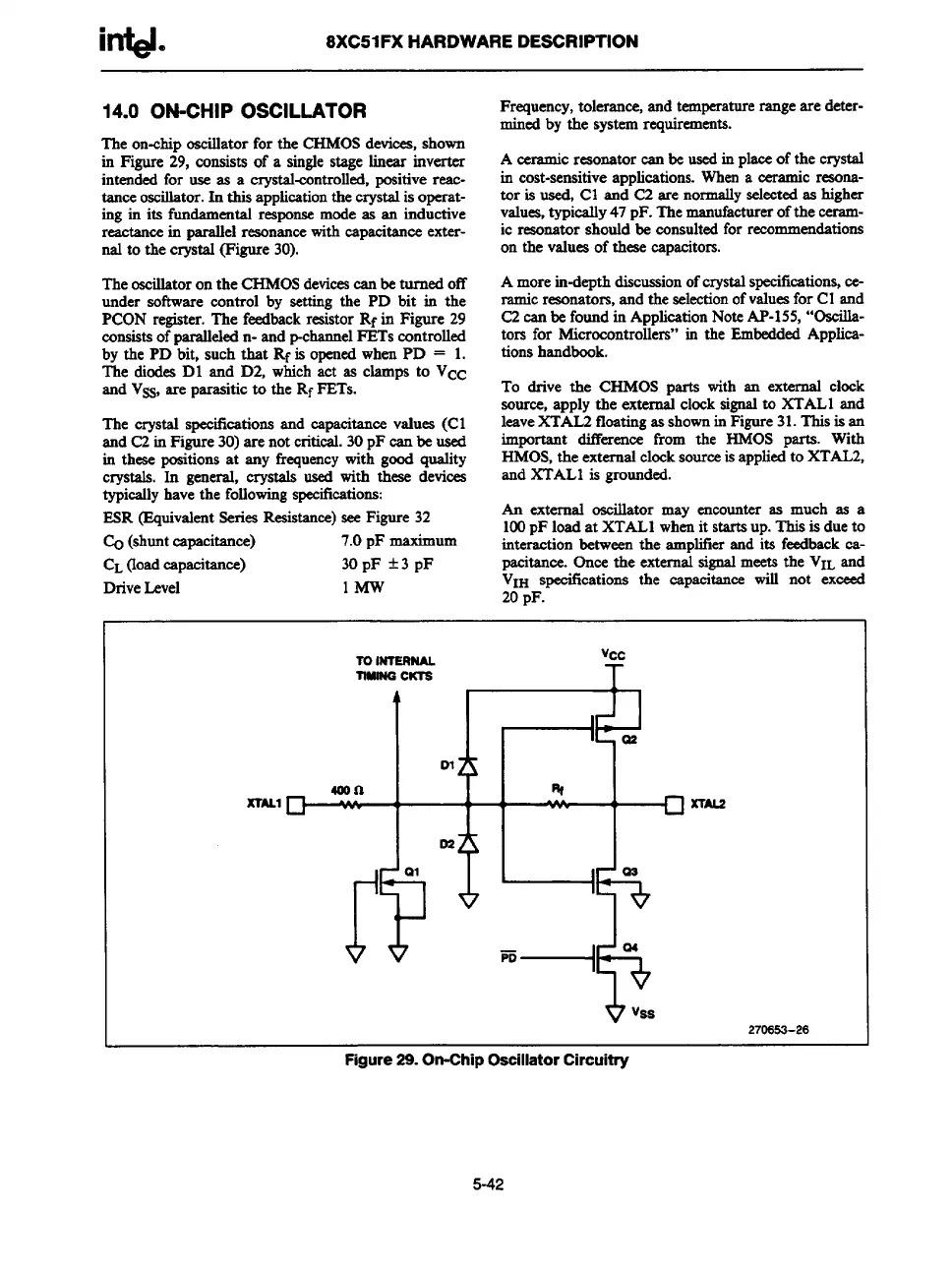
The on-chip oscillator for the CHMOS devices, shown
in Figure 29, consists of a single stage linear inverter
intended for use as a crystal-controlled,positive reac-
tance oscillator.In this applicationthe crystalis operat-
ing in its fimdamental response mode as an inductive
reactancein parallel resonancewith capacitance exter-
nal to the crystal (Figure 30).
The oscillatoron the CHMOS devicescan be turned off
under software control by setting the PD bit in the
PCON register.The feedbackresistor Rf in Figure 29
consists of paralleledn- and p-channelFETs controlled
by the PD bit, such that Rf is opened when PD = 1.
The diodes D1 and D2, which act as clamps to VcC
and V~, are parasitic to the Rf FETs.
The crystal specifications and capacitance valus (Cl
and C2 in Figure 30) arcnot critical.30 pF can be used
in these pesitions at any frequency with good quality
crystals. In general, crystals used with these devices
typically have the following specifications:
ESR (Equivalent Series Resistance)see Figure 32
~ (shunt capacitance)
7.0 pF
maximum
CL~OSdmptiti=)
30 pF *3 pF
Drive Level
lMW
Frequency, tolerance, and temperaturerangeare deter-
mined by the system requirements.
A ceramic resonatorcan be used in place of the crystal
in cost-sensitive applications. When a ceramic resona-
tor is us-ad,Cl and C2 are normally selected ss higher
values,typically 47 pF. The manufacturerof the ceram-
ic resonator should be consulted for recommendations
on the values of these capacitors.
A more in-depth discussion of crystalspecifications,ce-
ramicresonators,and the selectionofvalueafor Cl and
C2 can be found in Application Note AP-155, “Oscilla-
tors for Microcontrollers” in the Embedded Applica-
tions handbook.
To drive the CHMOS parts with an extemrd clock
source, apply the external ckwk signal to XTAL1 and
leaveXTAL2 floating as shown in Figure31. This is an
~po~t ~crcnce from the HMOS parts. With
HMOS, the external clock sourceis appliedto XTAL2,
and XTAL1 is grounded.
h external oscillator may encounter as much as a
100PF load at XTAL1 when it startsup. This is due to
inte~tion between the amplitier and ~ts feedback ca-
pacitance. Once the external signal meets the VIL and
VIH
specifications the capacitanm will not exceed
20 pF.
lo INTERNAL
Vcc
nNING Clcrs
T
ma
m
Xm.1
02
r?‘
;+
‘m+
F
1mm
XlU2
27066S-26
Figure 29. On-Chip Oscillator Circuitry
5-42