Library of Function Blocks
4.83
Function 37 - Digital Input with Timer Control (DIT)
Operation
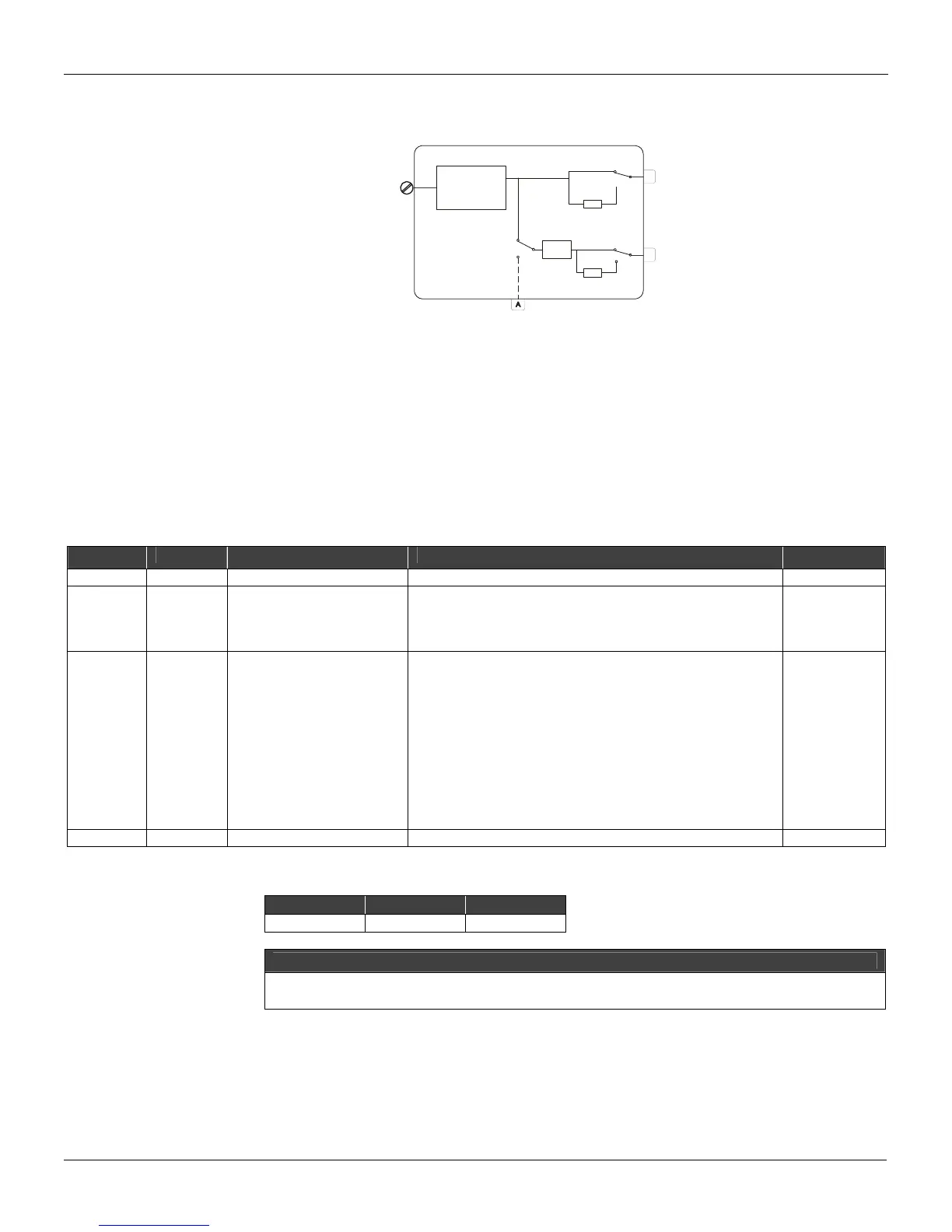
32/31/30/29
HIGH LEVEL
5 - 40V
OR OPEN CONTACT
171 / 173
175 / 177
0
CH1
BLK 122/123/124/125
1
0
CH2
NOT
1
0
1
172 / 174
176 / 178
TIME
DELAY
NOT
If the block terminal is open (impedance > 50 K
Ω) in relation to the Digital Ground or a 3 to 24 Vdc
voltage, the signal will be considered as a high logic level and the value of 100% (high logic level)
will be available at the output of the block.
If the input is short-circuited (impedance < 200
Ω) or its voltage is between 0 and 1.7 Vdc, the signal
will be considered low logic level and a 0% value on the output of the block.
This condition can be inverted by the
CNOT parameter.
This block also offers a delay on the digital signal, as defined on the
CACT parameter. This delay
time is through the
ADEL parameter.
TYPE MNEM DESCRIPTION RANGE DEFAULT
I LIA Input A
I CNOT Inverse switches
0 - Direct / Direct
1 - Inverse / Direct
2 - Direct / Inverse
3 - Inverse / Inverse
0
I CACT Actuation type
0 - None
1 – Delay for operation (Input connector)
2 – Delay for output (Input connector)
3 – Delay for output and operation (Input connector)
4 – Monostable Positive Transition (Input connector)
5 – Monostable Negative Transition (Input connector)
6 – Delay for operation (Input A)
7 Delay for output (Input A)
8 – Delay for output and operation (Input A)
9 – Monostable Positive Transition (Input A)
10 – Monostable Negative (Input A)
0
P ADEL Time delay 0.01 min to 180.00 min 1.00 min
Number of Bytes per Type of Parameter:
LINK CONF ADJ
2 4 2
NOTE
On the online change of the CACT parameter, it should be first changed to “0” and then, to the
desired value.