108 www.xilinx.com 7 Series FPGAs SelectIO Resources User Guide
UG471 (v1.10) May 8, 2018
Chapter 2: SelectIO Logic Resources
ILOGIC can support the following operations:
• Edge-triggered D-type flip-flop
• IDDR mode (OPPOSITE_EDGE or SAME_EDGE or SAME_EDGE_PIPELINED). See
Input DDR Overview (IDDR), page 109 for further discussion on input DDR.
• Level sensitive latch
• Asynchronous/combinatorial
The ILOGIC block registers have a common clock enable signal (CE1) that is active High by
default. If left unconnected, the clock enable pin for any storage element defaults to the
active state.
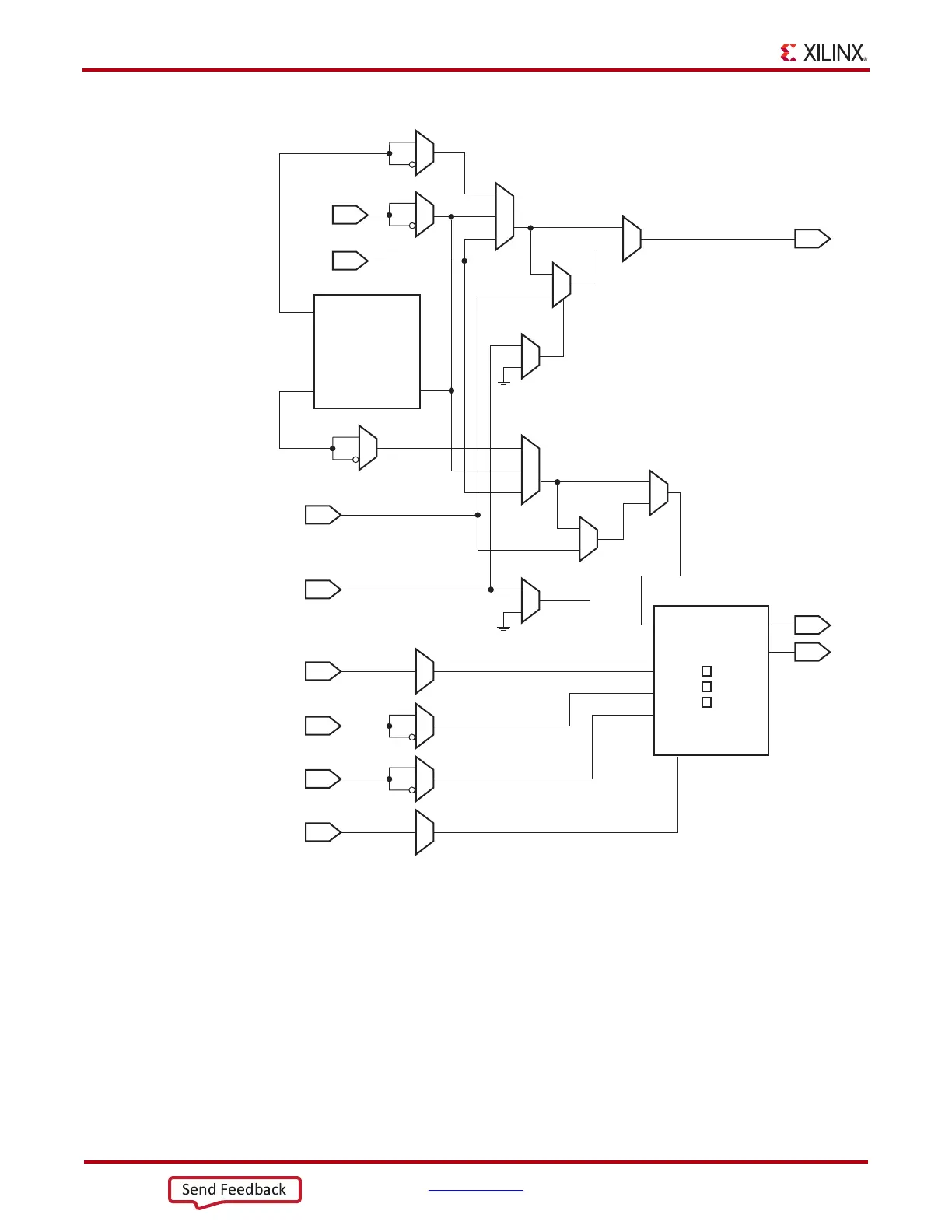
X-Ref Target - Figure 2-4
Figure 2-4: ILOGICE3 Block Diagram
UG471_c2_02_081215
O
ZHOLD_DELAY
D
DDLY
D
DLYFABRIC
DLVIFF
DLYIN
CE
CK
CKB
S/R
Q1
Latch
FF
DDR
Q2
OFB
TFB
CE1
CLK
CLKB
S/R
Q1
Q2