122 www.xilinx.com 7 Series FPGAs SelectIO Resources User Guide
UG471 (v1.10) May 8, 2018
Chapter 2: SelectIO Logic Resources
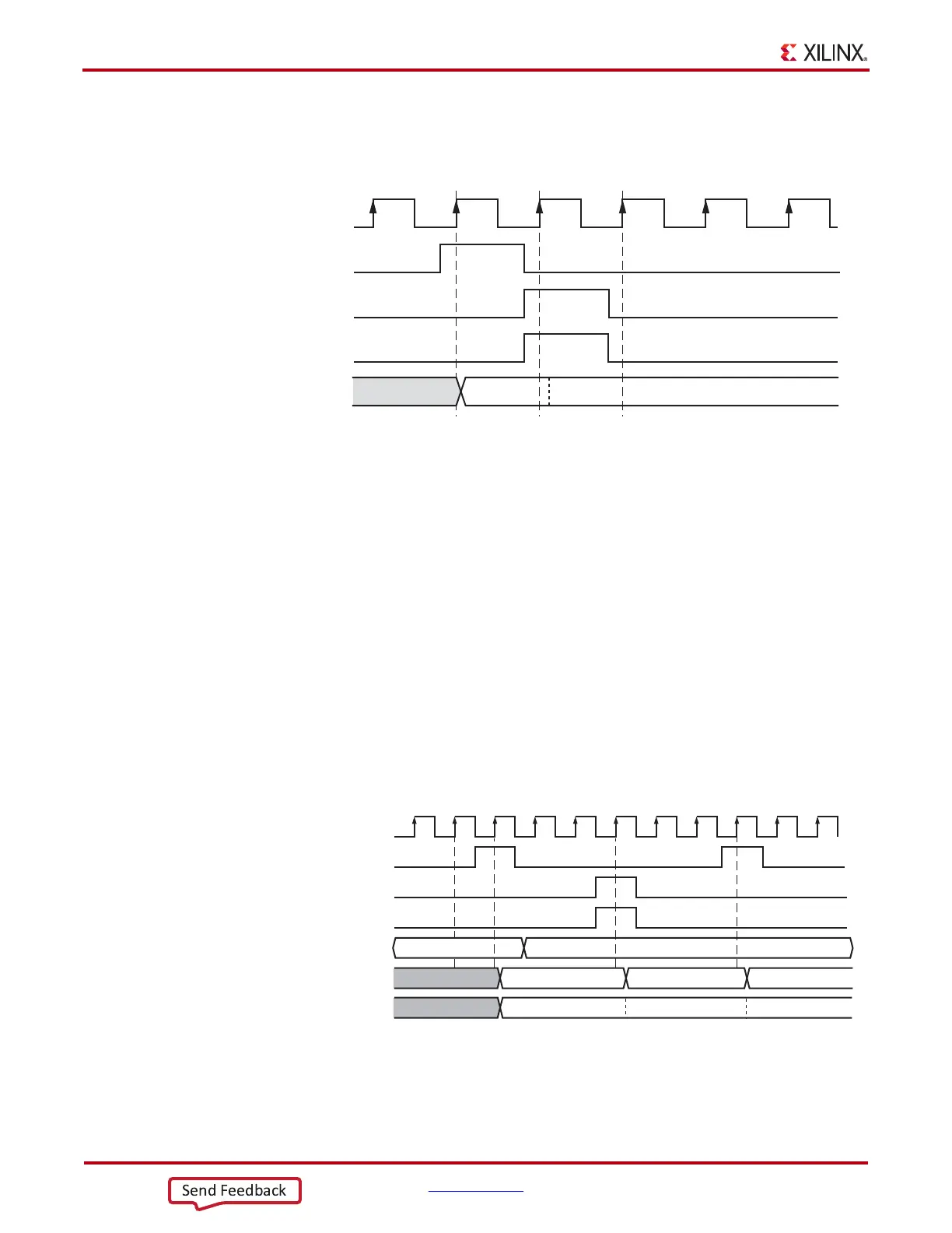
Figure 2-12 shows an IDELAY (IDELAY_TYPE = VARIABLE, IDELAY_VALUE = 0, and
DELAY_SRC = IDATAIN) timing diagram.
Clock Event 1
On the rising edge of C, a reset is detected (LD is High), causing the output DATAOUT to
select tap 0 as the output from the 31-tap chain.
Clock Event 2
A pulse on CE and INC is captured on the rising edge of C. This indicates an increment
operation. The output changes without glitches from tap 0 to tap 1. See Stability after an
Increment/Decrement Operation.
Clock Event 3
CE and INC are no longer asserted, thus completing the increment operation. The output
remains at tap 1 indefinitely until there is further activity on the LD, CE, or INC pins.
Figure 2-13 shows an IDELAY timing diagram in VAR_LOAD mode.
X-Ref Target - Figure 2-1 2
Figure 2-12: IDELAY Timing Diagram
X-Ref Target - Figure 2-1 3
Figure 2-13: IDELAY in VAR_LOAD Timing Diagram
UG471_c2_10_011811
LD
C
123
CE
INC
DATAO U T
Tap 0 Tap 1
C
LD
INC
CE
CNTVALUEIN
CNTVALUEOUT
DATAO UT
5’b00010 5’b00011 5’b01010
5’b00010 5’b01010
01 2 3
Tap 2 Tap 3 Tap 10
UG471_c2_11_011811