341
ABOV Semiconductor Co., Ltd.
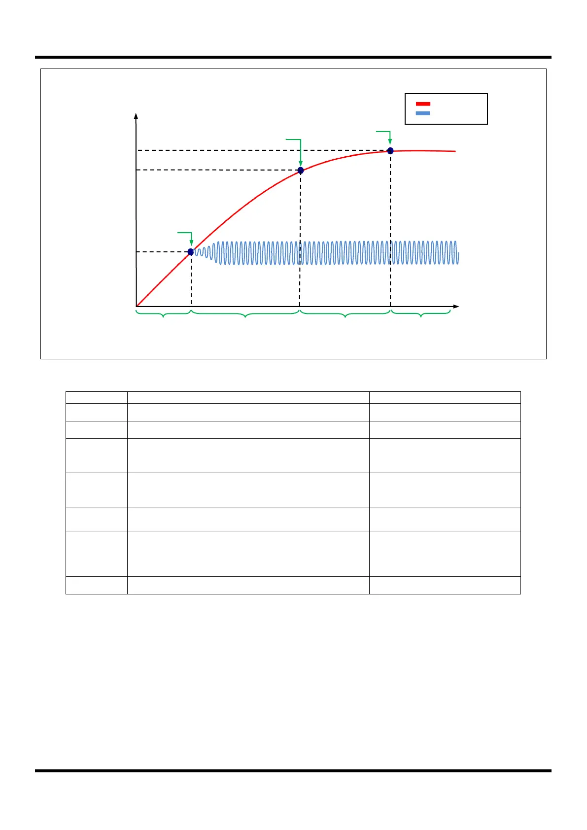
Figure 13.6 Boot Process WaveForm
-(INT-OSC 8MHz/8)x256x28h Delay section (=10ms)
-VDD input voltage must rise over than flash
operating voltage for Config read
-about 1.5V ~ 1.6V
-Config Value is determined by
Writing Option
- Rising section to Reset Release Level
-16ms point after POR or
Ext_reset release
- Reset Release section (BIT overflow)
i) after16ms, after External Reset Release (External
reset)
ii) 16ms point after POR (POR only)
- BIT is used for Peripheral
stability
Table 13-2 Boot Process Description