284
8331B–AVR–03/12
Atmel AVR XMEGA AU
When using 10-bit addressing, the address match logic only supports hardware address recog-
nition of the first byte of a 10-bit address. By setting ADDR[7:1] = 0b11110nn, ”nn” represents
bits 9 and 8 of the slave address. The next byte received is bits 7 to 0 in the 10-bit address, and
this must be handled by software.
When the address match logic detects that a valid address byte is received, APIF is set and the
DIR flag is updated.
If the PMEN bit in CTRLA is set, the address match logic responds to all addresses transmitted
on the TWI bus. The ADDR register is not used in this mode.
•Bit 0
– ADDR: General Call Recognition Enable
When ADDR[0] is set, this enables general call address recognition logic so the device can
respond to a general address call that addresses all devices on the bus.
21.10.5 DATA
– Data register
The data (DATA) register is used when transmitting and received data. During data transfer,
data are shifted from/to the DATA register and to/from the bus. This implies that the DATA regis-
ter cannot be accessed during byte transfers, and this is prevented by hardware. The DATA
register can be accessed only when the SCL line is held low by the slave; i.e., when CLKHOLD
is set.
When a master is reading data from the slave, data to send must be written to the DATA regis-
ter. The byte transfer is started when the master starts to clock the data byte from the slave,
followed by the slave receiving the acknowledge bit from the master. DIF and CLKHOLD are set.
When a master writes data to the slave, DIF and CLKHOLD are set when one byte has been
received in the DATA register. If smart mode is enabled, reading the DATA register will trigger
the bus operation as set by the ACKACT bit.
Accessing the DATA register will clear the slave interrupt flags and CLKHOLD. When an
address match occurs, the received address will be stored in the DATA register.
21.10.6 ADDRMASK
– Address Mask register
• Bit 7:1
– ADDRMASK[7:1]: Address Mask
These bits can act as a second address match register or as an address mask register, depend-
ing on the ADDREN setting.
If ADDREN is set to zero, ADDRMASK can be loaded with a 7-bit slave address mask. Each bit
in ADDRMASK can mask (disable) the corresponding address bit in the ADDR register. If the
Bit 76543210
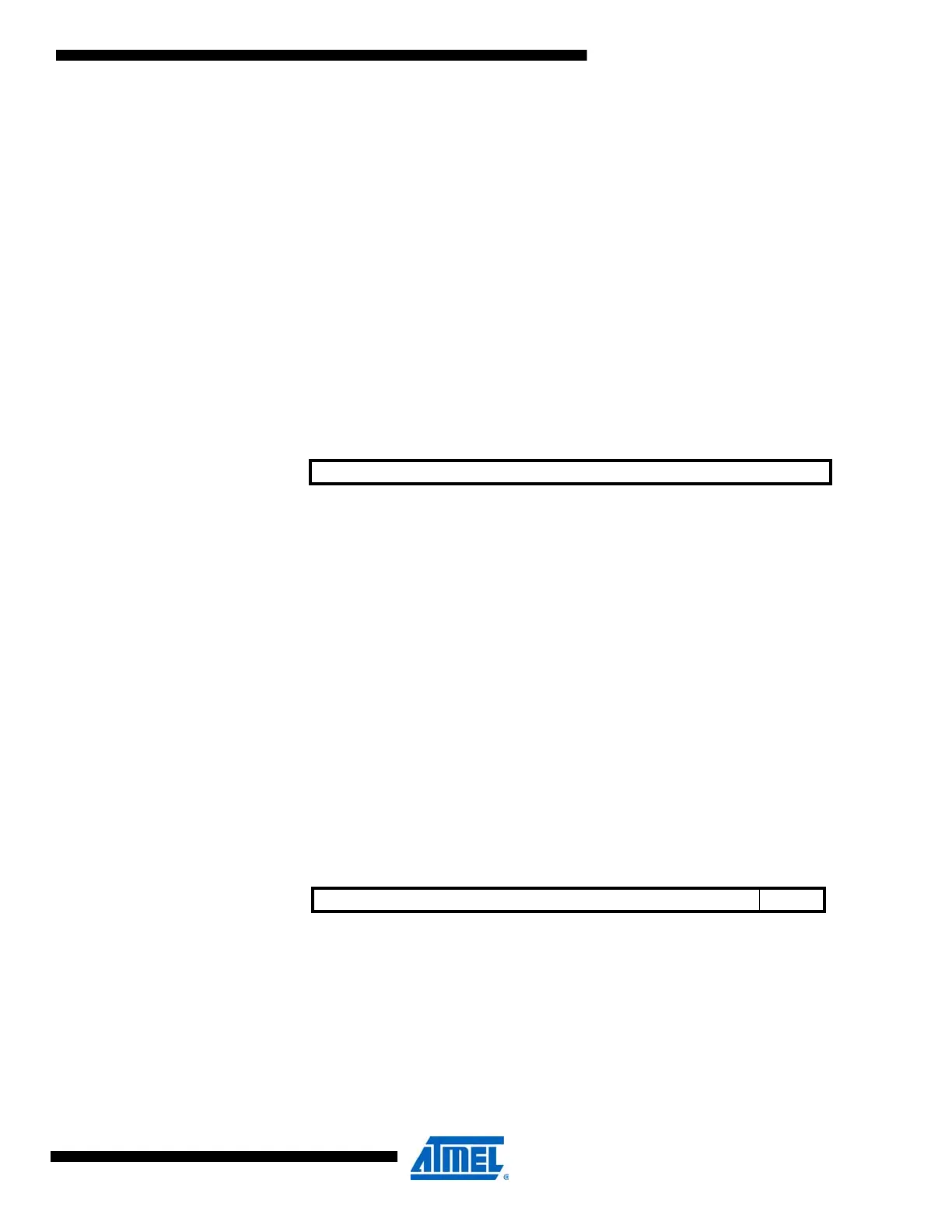
+0x04 DATA[7:0] DATA
Read/Write R/W R/W R/W R/W R/W R/W R/W R/W
Initial Value 0 0 0 0 0 0 0 0
Bit 76543210
+0x05 ADDRMASK[7:1] ADDREN ADDRMASK
Read/Write R/W R/W R/W R/W R/W R/W R/W R/W
Initial Value00000000
 Loading...