395
8331B–AVR–03/12
Atmel AVR XMEGA AU
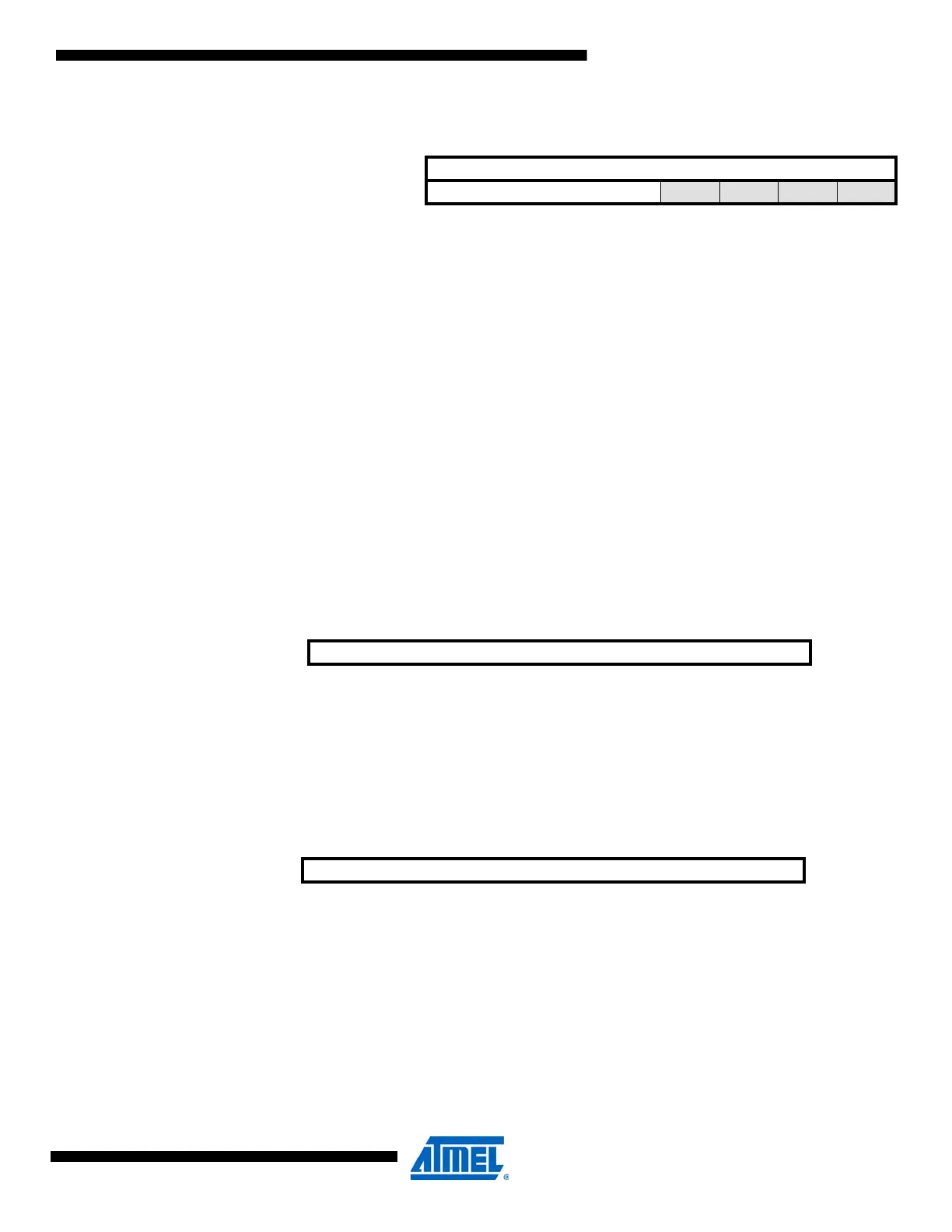
29.10.9 CH1DATAL – Channel 1 Data Register Low
29.10.9.1 Right-adjusted
• Bit 7:0 – CHDATA[7:0]: Conversion Data Register Channel 1, Eight lsbs
These bits are the eight lsbs of the 12-bit value to convert to channel 1 in right-adjusted mode.
29.10.9.2 Left-adjusted
• Bits 7:4 – CHDATA[3:0]: Conversion Data Register Channel 1, Four lsbs
These bits are the four lsbs of the 12-bit value to convert to channel 1 in left-adjusted mode.
• Bit 3:0 – Reserved
These bits are unused and reserved for future use. For compatibility with future devices, always
write these bits to zero when this register is written.
29.10.10 CH0GAINCAL – Gain Calibration Register
• Bit 7:0 – CH0GAINCAL[7:0]: Gain Calibration value
These bits are used to compensate for the gain error in DAC channel 0. See ”Calibration” on
page 388 for details.
29.10.11 CH0OFFSETCAL – Offset Calibration Register
• Bit 7:0 – CH1OFFSETCAL[7:0]: Offset Calibration value
These bits are used to compensate for the offset error in DAC channel 0. See ”Calibration” on
page 388 for details.
Bit 76543210
Right-adjust
+0x1A
CHDATA[7:0]
Left-adjust CHDATA[3:0] – – – –
Right-adjust Read/Write R/W R/W R/W R/W R/W R/W R/W R/W
Left-adjust Read/Write R/W R/W R/W R/W R R R R
Right-adjust Initial Value 0 0 0 0 0 0 0 0
Left-adjust Initial Value 0 0 0 0 0 0 0 0
Bit 76543210
+0x08 /+0x0A CH0GAINCAL[7:0] CH0GAINCAL
Read/Write R/W R/W R/W R/W R/W R/W R/W R/W
Initial Value00000000
Bit 76543210
+0x09 CH0OFFSETCAL[7:0] CH0OFFSETCAL
Read/Write R/W R/W R/W R/W R/W R/W R/W R/W
Initial Value00000000

 Loading...


