i~.
87C51GB HARDWARE DESCRIPTION
4.0
1/0 PORTS
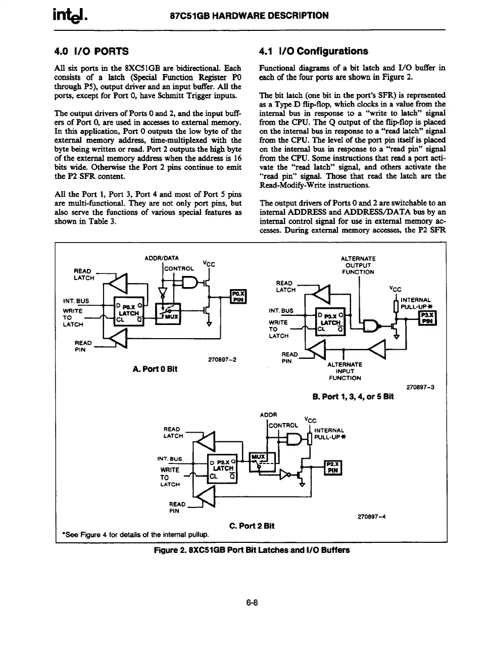
All six ports in the 8XC51GBare bidirectional.Each
consists of a latch (Special Frmction Register PO
throughP5), output driverend an input buffer.All the
ports, exceptfor Port O,haveSchmittTriggerinputs.
The outputdriversof Ports Oend2, end the inputbuff-
ers of Port O,are used in acceses
to externalmemory.
In this application,Port Ooutputsthe lowbyte of the
external memory address, time-multiplexedwith the
bytebeingwrittenor read. Port 2 outputsthe highbyte
of the externalmemoryaddresswhenthe addressis 16
bitswide.Otherwisethe Port 2 pins continueto emit
the P2 SFR content.
All thePort 1,Port 3,Port4 endmostofPort5 pins
aremulti-functional.T’heyarenotonly port pins, but
also serve the functionsof variousspecial features as
4.1 1/0 Configurations
Functionaldiagrams of a bit latch end 1/0 bufRwin
each ofthe four ports are shownin Figure2.
The bit latch (onebit in the port’sSFR)is represented
as a TypeD tliptlop, whichclocksin a valuefromthe
internal bus in response to a “write to latch” signal
fromthe CPU.The Q output of the flip-flopis placed
on the internalbus in responseto a “read latch” signaf
fromthe CPU.The levelof the port pinitselfis placed
on the internalbus in responseto a “read pin” signal
fromthe CPU.Someinstructionsthat read a port acti-
vate the “read latch” signal, end others activate the
“read pin” signal.Those that read the latch are the
Read-Modify-Writeinstructions.
TheoutputdriversofPortsOand 2are switchableto an
internalADDRESSand ADDRESS/DATAbusby an
shownin Table 3.
internal controlsignal for use in externalmemoryae-
ceses. Duringexternal memoryaccease$
the P2 SFR
ADDRIDATA
Vcc
ill%
CONTROL
.
Mux
u
Pe.x
pm
270897-2
tl.
PortII Bit
ALTERNATE
OUTPUT
FUNCTION
a
IN 1.BUS
D ~x au I
WRITE
LATCH
TO
CL
F
LATCH
““-:D*
ALTERNATE
INPUT
FUNCTION
270897-3
B. Port 1,3,4, or 5
Bit
ADDR
Vcc
REAO
CONTROL
LATCH
INT.BuS
WRITE
d
- CL
To
G
LATCH
READ
PIN
C.Port2 Bit
%eaFigure4fordetailsoftheinternalPUIIUP.
270897-4
Figure2.8XC51GBPortBitLatchesand1/()Buffers
6-8